 ALLPCB


Navigating the complexities of 12-layer PCB manufacturing can be daunting, especially when high reliability is a non-negotiable requirement. These multilayer boards are essential for advanced electronics in industries like aerospace, medical devices, and telecommunications, where performance and durability are critical. In this comprehensive guide, we’ll explore the 12-layer PCB manufacturing process, dive into the specific challenges of fabrication, and provide practical solutions to ensure your boards meet the highest standards of quality. Whether you're concerned about 12-layer PCB fabrication tolerances, drilling, plating, or lamination, we’ve got you covered with actionable insights.
What is a 12-Layer PCB and Why is it Important?
A 12-layer PCB is a printed circuit board with 12 distinct layers of conductive copper, separated by insulating materials, all stacked together to form a single, compact unit. These boards are designed to handle complex circuits with high-density interconnections, making them ideal for sophisticated applications. Think of advanced communication systems or critical medical equipment where space is limited, but functionality cannot be compromised.
The importance of a 12-layer PCB lies in its ability to support intricate designs while maintaining signal integrity and power distribution. However, with more layers comes greater complexity in manufacturing. Issues like misalignment, uneven plating, or thermal stress can compromise reliability. That’s why understanding the 12-layer PCB manufacturing process and addressing its challenges is crucial for engineers and designers aiming for flawless performance.
Key Stages in the 12-Layer PCB Manufacturing Process
The 12-layer PCB manufacturing process involves multiple stages, each with its own set of challenges. Below, we break down the critical steps, focusing on areas like drilling, plating, and lamination, while highlighting potential pitfalls and solutions for high-reliability boards.
1. Design and Stackup Planning
Before fabrication begins, a detailed design and stackup plan is created. A typical 12-layer PCB stackup might include alternating layers of copper foil (often 35μm thick after plating) and insulating prepreg materials like FR-4, which provide dielectric strength. The goal is to balance signal integrity, impedance control (often targeting values like 50 ohms for high-speed signals), and thermal management.
Challenge: Incorrect stackup design can lead to signal crosstalk or impedance mismatches, especially in high-speed applications where signal speeds exceed 1 GHz.
Solution: Use simulation tools to model signal behavior and adjust layer thickness or spacing. Ensure power and ground planes are positioned to minimize noise.
2. Material Selection for High Reliability
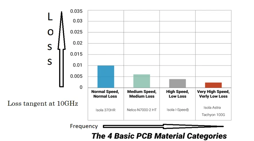
Choosing the right materials is vital for durability, especially for boards operating in harsh environments. Standard FR-4 might suffice for consumer electronics, but high-reliability applications often require advanced laminates with low dielectric loss (Df values below 0.005) and high thermal resistance (Tg above 170°C).
Challenge: Material mismatches can cause delamination or warping during thermal cycles.
Solution: Select materials with compatible coefficients of thermal expansion (CTE) and verify their performance through testing under simulated operating conditions.
3. 12-Layer PCB Drilling: Precision is Key
12-layer PCB drilling is a critical step where vias and through-holes are created to connect layers. With 12 layers, the board thickness can exceed 2.0 mm, requiring drills with diameters as small as 0.2 mm for microvias. Maintaining precision at this scale is essential to avoid misalignment.
Challenge: Drill wander or breakage can result in misaligned vias, disrupting connectivity. High aspect ratios (depth-to-diameter ratios above 10:1) increase the risk of defects.
Solution: Use advanced laser drilling for microvias to achieve tighter tolerances (down to ±0.05 mm). Employ automated optical inspection (AOI) to detect drilling errors early in the process.
4. 12-Layer PCB Plating: Ensuring Uniform Conductivity
After drilling, 12-layer PCB plating applies a conductive copper layer inside the vias and on the surface to ensure reliable electrical connections. Electroless copper deposition followed by electroplating is common, targeting a uniform thickness of 25-30μm inside vias.
Challenge: Uneven plating can lead to weak connections or voids, especially in deep vias. High layer count increases the risk of inconsistent current distribution during plating.
Solution: Optimize plating bath chemistry and use pulse plating techniques to improve uniformity. Implement strict process controls to monitor copper thickness with X-ray fluorescence (XRF) testing.
5. 12-Layer PCB Lamination: Bonding Layers Together
12-layer PCB lamination involves pressing the layers of copper and prepreg together under high temperature (around 180°C) and pressure (up to 500 psi). This step bonds the stackup into a single, cohesive board while maintaining alignment.
Challenge: Misalignment during lamination can shift layers, causing electrical shorts or open circuits. Thermal stress can also lead to warping or delamination.
Solution: Use precision alignment pins and controlled heating/cooling cycles to minimize stress. Post-lamination X-ray inspection can verify layer alignment within tolerances of ±0.1 mm.
6. Etching and Patterning for Circuit Definition
Once laminated, the copper layers are etched to create the desired circuit patterns. Photolithography defines the traces with line widths and spacing as tight as 0.075 mm for high-density designs.
Challenge: Over-etching or under-etching can result in trace defects, impacting signal integrity.
Solution: Fine-tune etching parameters and use automated inspection to ensure trace accuracy. Maintain cleanroom conditions to prevent contamination.
7. Final Assembly and Testing
After fabrication, the board undergoes solder mask application, surface finishing (like ENIG for corrosion resistance), and assembly. Rigorous testing, including electrical continuity checks and thermal cycling (from -40°C to 85°C), ensures reliability.
Challenge: Hidden defects like micro-cracks may only appear under stress, leading to field failures.
Solution: Perform in-circuit testing (ICT) and automated X-ray inspection (AXI) to detect subsurface issues. Subject boards to accelerated life testing to simulate long-term use.
12-Layer PCB Fabrication Tolerances: Meeting Precision Standards
12-layer PCB fabrication tolerances are a cornerstone of high-reliability manufacturing. With multiple layers, even small deviations can cascade into major issues. Here are the key tolerances to monitor and how to achieve them:
- Layer-to-Layer Registration: Target alignment within ±0.05 mm to prevent via misalignment. Use precision lamination and X-ray inspection.
- Drill Position Accuracy: Maintain tolerances of ±0.075 mm for via placement. Advanced CNC drilling machines with optical feedback help achieve this.
- Trace Width/Spacing: For high-density designs, aim for ±10% tolerance on trace widths (e.g., 0.1 mm traces within ±0.01 mm). Automated etching controls are essential.
- Board Thickness: Keep overall thickness within ±0.1 mm of the target (e.g., 2.0 mm) to ensure compatibility with enclosures. Controlled lamination pressure helps.
Tight tolerances demand advanced equipment and strict quality control. Partnering with a manufacturer that invests in precision technology and adheres to standards like IPC-6012 (Class 3 for high-reliability) can make all the difference.
Common Challenges in 12-Layer PCB Manufacturing and Solutions
Beyond the specific stages, broader challenges can impact the reliability of 12-layer PCBs. Here, we address these issues with practical solutions:
Signal Integrity and Crosstalk
With 12 layers, signals traveling at high speeds (above 1 GHz) are prone to interference and crosstalk, especially if power and signal layers are not properly isolated.
Solution: Design with dedicated ground planes adjacent to signal layers to reduce noise. Use controlled impedance routing with trace widths calculated for 50-ohm lines.
Thermal Management
High-density designs generate significant heat, and with 12 layers, heat dissipation becomes challenging, risking component failure.
Solution: Integrate thermal vias (0.3 mm diameter, spaced 1 mm apart) to transfer heat to outer layers. Consider metal-core substrates for extreme cases.
Manufacturing Cost and Lead Time
The complexity of 12-layer boards often results in higher costs and longer production times, which can strain budgets and deadlines.
Solution: Optimize designs for manufacturability (DFM) by minimizing via types and layer transitions. Collaborate with your manufacturer early to streamline the process.
Why High-Reliability Matters in 12-Layer PCB Applications
High-reliability 12-layer PCBs are non-negotiable in industries where failure is not an option. Consider these examples:
- Aerospace: Avionics systems rely on 12-layer boards for navigation and communication, operating in extreme conditions (-55°C to 125°C). A single failure could be catastrophic.
- Medical: Devices like MRI machines use multilayer boards for precise signal processing. Reliability ensures accurate diagnostics.
- Telecommunications: 5G infrastructure demands high-speed signal integrity, supported by complex PCBs with tight tolerances.
Manufacturing these boards with precision ensures they perform consistently, even under stress, protecting both end-users and brand reputation.
Partnering for Success in 12-Layer PCB Manufacturing
Achieving high-reliability in 12-layer PCB manufacturing requires more than just technical know-how—it demands collaboration. Work with a manufacturer that prioritizes quality control at every step, from drilling and plating to lamination. Look for capabilities like automated inspection, adherence to strict fabrication tolerances, and a commitment to testing protocols that match your application’s needs.
By understanding the challenges and implementing the solutions outlined above, you can ensure your 12-layer PCBs meet the highest standards. Whether you’re designing for cutting-edge technology or mission-critical systems, mastering the 12-layer PCB manufacturing process is the key to success.
Conclusion
Manufacturing a 12-layer PCB for high-reliability applications is a complex but achievable task. By addressing challenges in 12-layer PCB drilling, plating, lamination, and maintaining strict fabrication tolerances, you can create boards that perform flawlessly in demanding environments. This guide has walked you through the critical stages of the 12-layer PCB manufacturing process, offering practical solutions to common issues. With the right approach and partnership, your multilayer designs can power the next generation of innovation.


