 ALLPCB


In the fast-evolving world of electronics, PCB grounding remains a critical factor for ensuring signal integrity, reducing noise, and maintaining overall performance. As we look to the future, what are the key trends and innovations shaping PCB grounding? This blog dives deep into the advancements in advanced PCB technology, including flexible PCBs, 3D PCBs, embedded components, and high-density interconnect (HDI) designs, to explore how grounding techniques are adapting to the demands of future electronics.
At ALLPCB, we’re committed to staying ahead of the curve by embracing cutting-edge solutions for modern PCB challenges. Whether you’re an engineer designing compact wearable devices or high-speed communication systems, understanding the future of grounding will help you create more reliable and efficient products. Let’s explore the trends and innovations that are set to redefine PCB grounding in the coming years.
Why PCB Grounding Matters More Than Ever
Grounding in printed circuit boards (PCBs) is the foundation of electrical stability. It provides a reference point for voltage levels, minimizes electromagnetic interference (EMI), and prevents signal distortion. As electronic devices become smaller, faster, and more complex, the importance of effective grounding grows. High-speed signals, for instance, can reach frequencies of 10 GHz or more in modern communication systems, making even tiny grounding issues—like impedance mismatches as small as 0.1 ohms—capable of causing significant performance drops.
With the rise of future electronics, such as 5G networks, Internet of Things (IoT) devices, and autonomous systems, grounding must evolve to meet new challenges. Let’s break down the emerging trends in advanced PCB technology and how they influence grounding strategies.
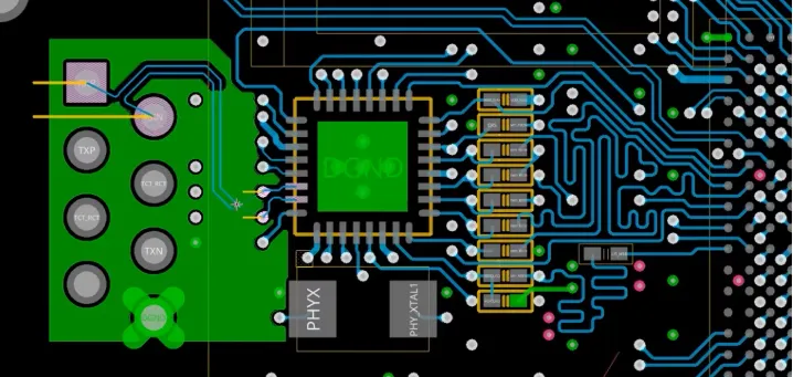
Trend 1: High-Density Interconnect (HDI) and Grounding Challenges
High-density interconnect (HDI) technology is a game-changer in PCB design, allowing for more components in smaller spaces through microvias and finer traces. HDI boards often feature trace widths as narrow as 3 mils (0.003 inches) and via diameters below 6 mils, enabling compact designs for smartphones, medical devices, and automotive systems. However, this density creates unique grounding challenges.
In HDI designs, the reduced space for ground planes can lead to higher impedance and increased noise. To counter this, engineers are adopting innovative grounding techniques, such as using multiple ground layers and stitching vias. Stitching vias, placed at intervals of less than 1/10th of the signal wavelength (e.g., every 3 mm for a 10 GHz signal), help create a low-impedance path for return currents, reducing EMI.
As HDI continues to dominate future electronics, grounding solutions will focus on optimizing layer stack-ups and via placement to maintain signal integrity even in the tightest layouts.
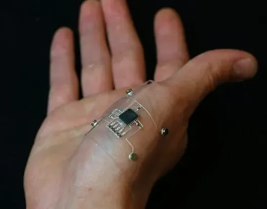
Trend 2: Flexible PCBs and Dynamic Grounding Solutions
Flexible PCBs are revolutionizing industries like wearables, aerospace, and medical technology by allowing circuits to bend and conform to unique shapes. These boards often use polyimide substrates with thicknesses as low as 1 mil (0.001 inches), offering incredible flexibility but complicating grounding.
Traditional rigid PCBs rely on large, continuous ground planes, but flexible PCBs often require segmented or meshed ground structures to maintain flexibility. This can increase ground impedance and noise, especially for high-frequency signals above 1 GHz. To address this, designers are exploring conductive adhesives and thin copper mesh layers to create effective grounding without sacrificing flexibility.
In the future, we expect to see more advancements in materials for flexible PCBs, such as conductive polymers, that enhance grounding performance while supporting the dynamic nature of these boards. This will be critical for next-generation wearables and foldable devices.
Trend 3: 3D PCBs and Grounding in Three Dimensions
3D PCBs, which stack multiple layers or use additive manufacturing to create three-dimensional circuit structures, are gaining traction for their ability to save space and improve performance. These designs are particularly useful in compact applications like drones and IoT sensors, where traditional planar PCBs are too bulky.
Grounding in 3D PCBs is far more complex than in 2D designs. The vertical interconnects and non-planar geometries can create uneven current distribution, leading to hotspots and signal interference. To tackle this, engineers are developing 3D grounding grids that wrap around components, ensuring a uniform reference plane across all dimensions. Some designs even integrate ground structures directly into the 3D-printed substrate, reducing impedance to below 0.05 ohms in critical areas.
As 3D printing technology advances, we anticipate more precise control over grounding structures, enabling seamless integration into complex, multi-dimensional layouts for future electronics.
Trend 4: Embedded Components and Grounding Integration
Embedding components like capacitors, resistors, and even ICs directly into the PCB substrate is a growing trend that reduces board size and improves performance. By placing components within the layers of the PCB, signal paths are shortened, often reducing trace lengths by 50% or more, which minimizes parasitic inductance and enhances speed.
However, embedded components pose grounding challenges. Without proper isolation, these components can interfere with ground planes, creating noise and reducing effectiveness. Innovative solutions include dedicated ground cavities around embedded components and the use of buried vias to connect directly to ground layers. These techniques ensure that return currents have a clear, low-impedance path, even in densely packed designs.
The future of embedded components will likely involve smarter integration with grounding structures, using advanced materials and design tools to balance compactness with electrical stability.
Trend 5: Advanced Materials for Grounding in Future Electronics
The materials used in PCB manufacturing are evolving to meet the demands of high-speed and high-frequency applications. Traditional FR-4 substrates, with a dielectric constant of around 4.5, often struggle with signal loss at frequencies above 5 GHz. New materials like low-loss laminates and ceramics, with dielectric constants as low as 2.2, are becoming more common in advanced PCB technology.
These materials not only improve signal integrity but also enhance grounding by reducing parasitic capacitance between ground planes and traces. Additionally, conductive coatings and graphene-based materials are being researched for their potential to create ultra-thin, highly conductive ground layers. Such innovations could lower ground impedance to below 0.01 ohms, a significant improvement over traditional copper planes.
As material science progresses, we expect grounding solutions to become more efficient, supporting the performance needs of future electronics like 6G networks and quantum computing systems.
Trend 6: AI and Simulation in Grounding Design
Artificial Intelligence (AI) and simulation tools are transforming how engineers approach PCB grounding. These technologies can analyze complex designs, predict EMI issues, and optimize ground plane layouts in a fraction of the time it takes for manual design. For instance, AI-driven software can simulate return current paths for a 10-layer HDI board in under an hour, identifying potential impedance issues down to 0.001 ohms.
In the future, AI will play an even larger role in grounding for flexible PCBs, 3D PCBs, and HDI designs. By integrating real-time data from manufacturing processes, these tools will enable adaptive grounding designs that adjust to specific environmental or operational conditions, ensuring optimal performance in dynamic systems.
The Role of Grounding in Sustainable PCB Design
Sustainability is becoming a priority in the electronics industry, and grounding plays a subtle but important role. Efficient grounding reduces power loss and heat generation, which can lower energy consumption in devices. For example, a well-designed ground plane can decrease power dissipation by up to 10% in high-speed circuits operating at 3.3V.
Moreover, as the industry moves toward green manufacturing, grounding designs are being optimized to work with eco-friendly materials and processes. This ensures that future electronics are not only high-performing but also environmentally responsible.
How ALLPCB Supports the Future of Grounding
At ALLPCB, we’re dedicated to helping engineers navigate the complexities of modern PCB design, including grounding for advanced applications. Our state-of-the-art manufacturing capabilities support HDI, flexible PCBs, and innovative 3D structures, ensuring that your grounding designs are implemented with precision. We also offer access to the latest materials and design tools to keep your projects at the forefront of technology.
Whether you’re working on compact IoT devices or high-speed communication systems, our team is ready to provide tailored solutions that meet the demands of future electronics. With a focus on quality and innovation, we’re here to support your journey into the next era of PCB technology.
Conclusion: Preparing for the Future of PCB Grounding
The future of PCB grounding is full of exciting possibilities, driven by trends in advanced PCB technology like HDI, flexible PCBs, 3D PCBs, and embedded components. As devices become smaller, faster, and more complex, grounding techniques must adapt to ensure reliability and performance. From new materials that reduce impedance to AI-driven design tools that optimize layouts, the innovations in grounding are set to transform future electronics.
By staying informed about these trends, engineers can design PCBs that meet the challenges of tomorrow’s applications. At ALLPCB, we’re proud to be part of this journey, offering the tools and expertise needed to bring your ideas to life. Let’s build the future of electronics together, one well-grounded design at a time.


