 ALLPCB


If you're looking for a comprehensive resource on the PCB prototyping assembly process, from creating a functional PCB prototype to mastering PCB design for assembly, prototype testing methods, and PCB prototype validation, you're in the right place. This guide walks you through every step, offering practical insights and actionable tips to help you turn your ideas into reality. Whether you're an engineer, designer, or hobbyist, we'll break down the complex process into manageable steps to ensure your prototype is ready for testing and production.
In the following sections, we'll dive deep into the entire journey of PCB prototyping assembly. You'll learn how to design with assembly in mind, assemble your prototype efficiently, and validate its functionality through proven testing methods. Let's get started on building a prototype that works flawlessly!
What Is PCB Prototyping Assembly and Why Does It Matter?
PCB prototyping assembly is the process of designing, fabricating, and assembling a printed circuit board (PCB) as a working model before mass production. This step is crucial because it allows you to test your design, identify errors, and make improvements without the high costs of full-scale manufacturing. A functional PCB prototype acts as proof of concept, ensuring that your circuit performs as expected under real-world conditions.
The importance of prototyping cannot be overstated. According to industry studies, up to 70% of electronic product failures can be traced back to design flaws that could have been caught during the prototyping phase. By investing time and effort into a well-executed prototype, you save resources and reduce the risk of costly redesigns later. This guide will cover every aspect of the process, focusing on long-tail keywords like PCB prototyping assembly process, functional PCB prototype, and PCB design for assembly to ensure you have all the tools you need.
Step 1: PCB Design for Assembly – Laying the Foundation
The first step in creating a functional PCB prototype is designing the board with assembly in mind. PCB design for assembly (DFA) focuses on making the board easy to manufacture and assemble, reducing errors and costs. A poorly designed PCB can lead to issues like misaligned components, signal interference, or even complete failure during testing.
Here are key considerations for effective PCB design:
- Component Placement: Place components logically to minimize trace lengths and avoid overcrowding. For high-speed circuits, keep critical components close to reduce signal delay. For instance, in a design with a 100 MHz clock signal, keeping traces under 1 inch can help maintain signal integrity.
- Trace Width and Spacing: Ensure traces are wide enough to handle the current without overheating. A common guideline is to use a trace width of 10 mils for signals carrying up to 1 amp. Spacing between traces should also prevent crosstalk, especially for high-frequency designs.
- Layer Stack-Up: For complex designs, use multiple layers to separate power, ground, and signal planes. A 4-layer board with dedicated ground and power planes can reduce noise by up to 30% compared to a 2-layer board.
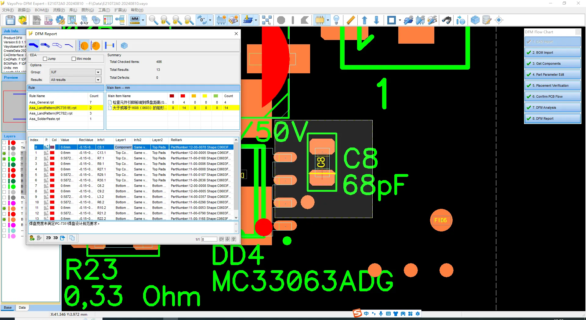
- Design Rule Checks (DRC): Use design software to run DRCs and catch errors like unconnected pins or overlapping traces before sending your design for fabrication.
By focusing on these elements, you ensure your PCB is ready for the assembly phase, minimizing rework and delays. A well-thought-out design is the backbone of a functional PCB prototype.
Step 2: The PCB Prototyping Assembly Process – Bringing Your Design to Life
Once your design is finalized, the next step is the PCB prototyping assembly process. This involves fabricating the bare board and assembling components onto it. The goal is to create a working prototype that can be tested for functionality. Here's how the process typically unfolds:
1. Fabrication of the Bare Board
Send your design files (often in Gerber format) to a fabrication service to create the bare PCB. The board is made by etching copper layers on a substrate like FR-4, which is a common material due to its durability and cost-effectiveness. Fabrication can take anywhere from 24 hours to a week, depending on complexity and turnaround time.
2. Sourcing Components
While the board is being fabricated, source the components listed in your Bill of Materials (BOM). Ensure components match the specifications in your design, such as resistor values (e.g., 1 kΩ ±5%) or capacitor ratings (e.g., 10 μF at 16V).
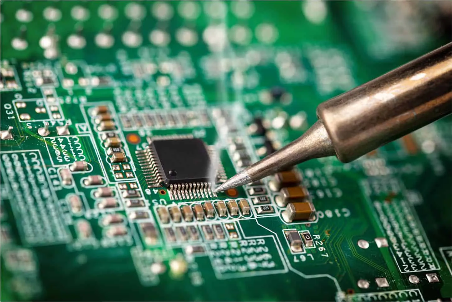
3. Assembly of Components
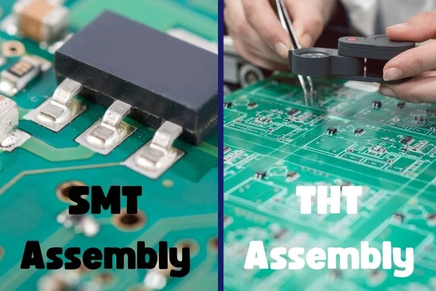
Assembly can be done manually for small batches or using automated machines for precision. Surface-mount technology (SMT) is common for modern prototypes due to its compact size. For example, an 0805 SMD resistor is just 2 mm long, allowing for dense layouts. Soldering techniques like reflow soldering ensure components are securely attached without damaging the board.
4. Initial Inspection
After assembly, inspect the board for soldering defects like cold joints or bridges. Use a magnifying glass or automated optical inspection (AOI) tools to spot issues. A single misplaced component can cause a short circuit, leading to prototype failure.
By carefully following these steps, you create a prototype ready for testing. The PCB prototyping assembly process is a critical bridge between design and validation, ensuring your board is functional before moving forward.
Step 3: Prototype Testing Methods – Ensuring Functionality
With your functional PCB prototype assembled, it's time to test it using proven prototype testing methods. Testing verifies that the board performs as intended and identifies any design or assembly flaws. Here are the most effective testing methods to apply:
1. Visual Inspection
Start with a thorough visual check for physical defects. Look for misaligned components, solder bridges, or damaged traces. This basic step can catch up to 50% of assembly issues before powering up the board.
2. Continuity Testing
Use a multimeter to check for continuity between points on the board. This ensures there are no open circuits or unintended shorts. For example, if a trace is supposed to connect a microcontroller pin to a sensor but shows no continuity, you’ve identified a potential fabrication error.
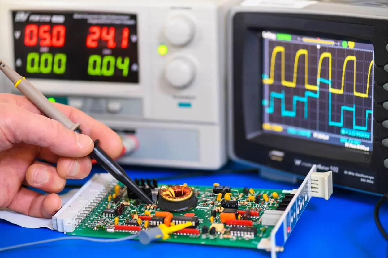
3. Power-On Testing
Apply power to the board and measure key parameters like voltage and current at specific points. If your design includes a 5V regulator, confirm the output is within ±0.1V of the target. Deviations could indicate a faulty component or design error.
4. Functional Testing
Test the board under real-world conditions to see if it performs its intended function. For a prototype controlling a motor, verify that the motor spins at the correct speed (e.g., 1000 RPM) when triggered. Use oscilloscopes to monitor signal integrity, especially for high-speed designs where noise can degrade performance.
5. Environmental Testing
Expose the prototype to conditions like temperature extremes or humidity to simulate operating environments. If your board is designed for outdoor use, test it at temperatures from -20°C to 60°C to ensure components don’t fail under stress.
These prototype testing methods help you catch issues early, ensuring your PCB prototype is reliable and ready for further validation.
Step 4: PCB Prototype Validation – Confirming Readiness for Production
The final step is PCB prototype validation, where you confirm that your design meets all requirements and is ready for mass production. Validation goes beyond basic testing to ensure long-term reliability and manufacturability. Here's how to approach it:
1. Design Verification
Compare the prototype’s performance against your original specifications. If your design required a signal-to-noise ratio (SNR) of 60 dB, measure the actual SNR using testing equipment. Any deviation means you need to revisit the design phase.
2. Stress Testing
Push the prototype beyond normal operating conditions to identify weak points. For instance, if your board is rated for 12V, test it at 15V to see if components overheat or fail. This helps uncover potential issues that might arise during long-term use.
3. Manufacturability Assessment
Evaluate whether the prototype can be scaled for production. Check if component placement allows for automated assembly and if tolerances (e.g., ±0.1 mm for hole sizes) are achievable in bulk manufacturing. A design that’s too complex may drive up costs unnecessarily.
4. Iterative Improvements
Based on validation results, make necessary adjustments. This might involve rerouting traces to reduce impedance (e.g., from 100 ohms to 50 ohms for better signal matching) or swapping out components for more reliable alternatives. Each iteration brings you closer to a production-ready design.
PCB prototype validation ensures that your design isn’t just functional in the lab but also practical for real-world applications and large-scale production.
Common Challenges in PCB Prototyping Assembly and How to Overcome Them
Even with careful planning, challenges can arise during the PCB prototyping assembly process. Here are some common issues and solutions:
- Component Misalignment: Misplaced components can lead to shorts or open circuits. Use precise placement tools or automated assembly to reduce errors. Double-check footprints in your design software before fabrication.
- Signal Integrity Issues: High-speed designs often suffer from crosstalk or noise. Minimize trace lengths and use ground planes to shield signals. For a 200 MHz signal, keeping traces under 0.5 inches can significantly reduce interference.
- Soldering Defects: Cold joints or bridges can cause intermittent failures. Use proper soldering techniques and inspect joints under magnification. Reflow soldering ovens can improve consistency for SMT components.
- Cost Overruns: Prototyping can become expensive with multiple iterations. Optimize your design early using simulation tools to predict performance and reduce the number of physical prototypes needed.
By anticipating these challenges, you can streamline the process and achieve a functional PCB prototype with fewer setbacks.
Conclusion: Mastering the Journey from Design to Functional Prototype
Creating a functional PCB prototype is a multi-step journey that requires attention to detail, from PCB design for assembly to the PCB prototyping assembly process, prototype testing methods, and PCB prototype validation. Each phase builds on the last, ensuring your design evolves from a concept into a reliable, production-ready board.
By following the steps outlined in this guide, you can avoid common pitfalls, save time, and reduce costs. Whether you're working on a simple circuit or a complex multi-layer board, the principles of careful design, thorough testing, and rigorous validation will lead to success. With a well-executed prototype, you're one step closer to bringing your innovative ideas to the market.
At ALLPCB, we're committed to supporting you through every stage of this process. Our expertise and resources are here to help you create high-quality prototypes that meet your needs. Start your journey today and turn your designs into reality with confidence!


