 ALLPCB


If you're searching for guidance on SMD inductor footprint guidelines, inductor PCB layout best practices, or surface mount inductor footprint design, you're in the right place. This blog post will provide a clear roadmap to designing effective SMD inductor footprints and layouts that ensure optimal performance and reliability for your printed circuit board (PCB) projects. We'll dive into the essentials of footprint design, layout considerations, and practical tips to help you avoid common pitfalls. Let’s explore how to achieve a robust and efficient design for your next project.
Introduction to SMD Inductors and Their Importance in PCB Design
Surface-mount device (SMD) inductors are critical components in modern electronics, used for energy storage, filtering, and noise suppression in circuits like power supplies and RF applications. Unlike through-hole components, SMD inductors are soldered directly onto the PCB surface, making their footprint design and placement vital for performance, manufacturability, and reliability. A poorly designed footprint or layout can lead to issues like signal interference, overheating, or even component failure. By following proper SMD inductor footprint guidelines and inductor PCB layout best practices, you can ensure your design meets both functional and production requirements.
In this comprehensive guide, we'll walk through the key aspects of surface mount inductor footprint design, from understanding package types to optimizing pad layouts and placement strategies. Whether you're a beginner or an experienced engineer, these insights will help you create designs that perform reliably under various conditions.
Understanding SMD Inductor Packages and Footprints
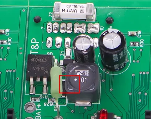
SMD inductors come in a variety of package sizes, often less standardized than other components like resistors or capacitors. Common package sizes are denoted by codes like 0402, 0603, or 0805, which represent dimensions in inches (e.g., 0402 is 0.04" x 0.02"). However, the exact footprint for an inductor depends on the manufacturer's datasheet, as pad spacing and dimensions can vary even within the same package size.
The footprint of an SMD inductor includes the copper pads where the component is soldered, along with solder mask and paste layers. A well-designed footprint ensures proper soldering during assembly, minimizes parasitic effects, and prevents mechanical stress on the component. When designing, always refer to the recommended land pattern in the inductor’s datasheet. If a matching footprint isn’t available in your PCB design software library, modify an existing one to match the datasheet dimensions—a process that typically takes just a few minutes.
For example, a typical 0603 inductor might have a pad width of 0.8 mm and a pad spacing of 1.6 mm, but these values can differ by manufacturer. Following SMD inductor footprint guidelines ensures compatibility with automated assembly processes and reduces the risk of soldering defects like tombstoning, where one end of the component lifts off the pad.
Key SMD Inductor Footprint Guidelines
Designing an effective footprint for SMD inductors requires attention to detail. Here are some essential guidelines to follow for surface mount inductor footprint design:
- Pad Dimensions: Match the pad size and spacing to the manufacturer’s recommendations. Pads that are too small can lead to poor solder joints, while overly large pads may cause excess solder to create shorts.
- Solder Mask and Paste: Ensure the solder mask opening is slightly larger than the pad to allow for proper soldering. The solder paste stencil should align with the pad area to deposit the correct amount of solder—typically covering 90-100% of the pad surface for small components.
- Clearance: Maintain adequate clearance between pads and nearby traces or components to prevent short circuits. A minimum clearance of 0.2 mm is often recommended for small inductors, though this can vary based on design rules.
- Thermal Relief: For inductors in high-current applications, consider adding thermal relief patterns to pads connected to large copper planes. This prevents heat dissipation issues during soldering, ensuring a reliable joint.
- Standards Compliance: Adhere to industry standards like IPC-7351, which provides detailed specifications for SMD footprints. This standard helps ensure manufacturability and consistency across designs.
By applying these SMD inductor footprint guidelines, you create a foundation for a reliable PCB design that performs well during both assembly and operation.
Inductor PCB Layout Best Practices for Optimal Performance
Beyond footprint design, the placement and routing of SMD inductors on a PCB significantly impact circuit performance. Inductors are often used in sensitive applications like switching regulators, where improper layout can introduce noise, electromagnetic interference (EMI), or efficiency losses. Below are some inductor PCB layout best practices to follow:
1. Placement Near Related Components
Place inductors close to the components they interact with, such as ICs in a switching regulator circuit. For example, in a buck converter, position the inductor near the switching node to minimize the length of high-current loops. Shorter loops reduce parasitic inductance and EMI. A typical guideline is to keep the distance between the inductor and the switching IC under 10 mm for high-frequency designs (above 1 MHz).
2. Minimize Loop Areas
In switching power supplies, the current loop involving the inductor, input capacitor, and output capacitor should be as small as possible. Large loop areas act as antennas, radiating EMI that can interfere with nearby circuits. Route traces on the same layer whenever possible, and use vias sparingly to avoid adding inductance. For a 2-layer board, aim for loop areas under 100 mm2 for frequencies around 500 kHz.
3. Ground Plane Considerations
Ground planes are essential for noise reduction, but their placement under inductors requires caution. For switching regulators, avoid placing a ground plane directly beneath the inductor or switching node, as it can couple noise into the ground. Instead, place the ground plane on an adjacent layer or offset it from high-noise areas. If a ground plane is unavoidable, use a cutout or split plane to isolate sensitive areas.
4. Orientation for EMI Reduction
Inductors generate magnetic fields that can interfere with nearby components or traces. Orient inductors to minimize field coupling—for instance, place them perpendicular to sensitive signal traces. In multi-inductor designs, space them at least 5-10 mm apart to reduce mutual interference, especially for inductors operating at similar frequencies.
5. Thermal Management
Inductors in power applications can generate significant heat, especially at high currents (e.g., above 2 A). Ensure adequate copper area around pads to dissipate heat, and avoid placing inductors near heat-sensitive components. If using a multilayer board, add thermal vias near the inductor pads to transfer heat to inner layers, keeping temperatures below the component’s rated limit (often 125°C).
Common Challenges in SMD Inductor Layout and How to Address Them
Even with careful planning, challenges can arise when designing with SMD inductors. Here are some common issues and solutions to ensure reliability:
- Parasitic Effects: Long traces or large loop areas introduce parasitic inductance and capacitance, degrading performance. Keep traces short and direct, especially for high-frequency circuits above 1 MHz, where even a 5 mm trace can add significant inductance (around 5 nH).
- Soldering Defects: Incorrect pad sizes or solder paste application can cause defects like tombstoning or weak joints. Double-check footprint dimensions against the datasheet, and ensure reflow profiles match the component’s requirements (e.g., peak temperature of 260°C for lead-free solder).
- Mechanical Stress: SMD inductors can crack under mechanical stress during board flexing. Place inductors away from board edges or high-stress areas, and consider adding underfill for extra support in rugged applications.
- EMI Issues: Magnetic fields from inductors can induce noise in nearby circuits. Use shielding if necessary, or increase spacing between inductors and sensitive components to at least 10 mm for designs with currents above 1 A.
Addressing these challenges during the design phase saves time and cost by preventing rework or field failures. Always simulate your layout for EMI and thermal performance if possible, using tools available in most PCB design software.
Tools and Standards for SMD Inductor Footprint Design
Creating accurate footprints and layouts is easier with the right tools and standards. Many PCB design platforms offer libraries with pre-defined SMD footprints, but these must be verified against the component datasheet. If customization is needed, use the footprint editor to adjust pad sizes, spacing, and layer settings to match surface mount inductor footprint design requirements.
The IPC-7351 standard is a valuable resource for footprint design. It provides detailed guidelines on pad shapes, sizes, and tolerances for various SMD components, including inductors. Following this standard ensures your design is compatible with automated assembly processes and meets industry expectations for reliability.
Additionally, consider using simulation tools to analyze EMI and thermal behavior before finalizing your layout. These tools can predict potential issues, such as noise coupling or hot spots, allowing you to make adjustments early in the design process.
Tips for Selecting the Right SMD Inductor for Your Design
Footprint and layout optimization go hand-in-hand with choosing the right inductor. Here are some factors to consider when selecting an SMD inductor:
- Current Rating: Choose an inductor with a current rating at least 20-30% higher than your circuit’s maximum current to prevent saturation. For example, a 1 A circuit should use an inductor rated for at least 1.3 A.
- Inductance Value: Match the inductance to your application—higher values (e.g., 10 μH) for low-frequency power supplies, and lower values (e.g., 1 μH) for high-frequency switching.
- DC Resistance (DCR): Select inductors with low DCR (e.g., below 50 mΩ) for power applications to minimize losses and heat generation.
- Package Size: Ensure the package fits your board’s space constraints while providing adequate pad area for soldering. Smaller packages like 0402 are ideal for compact designs but may have lower current ratings.
Balancing these factors with inductor PCB layout best practices ensures your design achieves both performance and reliability goals.
Conclusion: Building Better PCB Designs with Optimized SMD Inductor Layouts
Designing SMD inductor footprints and layouts is a critical step in creating high-performing, reliable PCBs. By adhering to SMD inductor footprint guidelines, following inductor PCB layout best practices, and focusing on precise surface mount inductor footprint design, you can minimize issues like EMI, thermal stress, and soldering defects. From selecting the right component to optimizing placement and routing, every decision impacts the final outcome of your design.
Take the time to review manufacturer datasheets, adhere to industry standards like IPC-7351, and simulate your layout for potential issues. With these strategies, you'll be well-equipped to tackle the challenges of modern PCB design and deliver circuits that meet the demands of today’s compact, high-performance electronics.
Start applying these principles in your next project, and watch as your designs achieve new levels of efficiency and durability. For more resources on PCB design and component selection, stay tuned to our blog for the latest tips and insights.


