 ALLPCB


If you're an electrical engineer looking to improve efficiency in your PCB assembly process, maximizing first pass yield (FPY) in wave soldering is a critical goal. How can you achieve higher FPY and reduce rework and waste? The answer lies in optimizing your wave soldering process through precise control of parameters, defect prevention strategies, and robust quality control measures. In this blog, we'll dive deep into actionable strategies for wave soldering first pass yield improvement, process optimization, defect reduction, and quality control to help you streamline production and cut costs.
What Is First Pass Yield in Wave Soldering and Why Does It Matter?
First Pass Yield (FPY) is a key metric in manufacturing that measures the percentage of units that pass through a process without needing rework or repair on the first attempt. In wave soldering—a bulk soldering process used to attach through-hole components to printed circuit boards (PCBs)—FPY directly impacts production efficiency, material costs, and overall product quality.
A low FPY means more boards fail inspection due to defects like insufficient solder, bridging, or cold joints, leading to costly rework and wasted resources. For electrical engineers, achieving a high FPY (ideally above 95%) is essential to meet tight production schedules and maintain profitability. Let’s explore how to optimize the wave soldering process to hit these targets.
Understanding Common Wave Soldering Defects Impacting FPY
Before diving into improvement strategies, it’s crucial to identify the common defects that lower FPY in wave soldering. By understanding these issues, you can target specific areas for optimization. Here are the primary defects:
- Insufficient Solder: Occurs when solder fails to fully wet the component leads or pads, often due to poor fluxing, low solder temperature, or contamination on the board. This can lead to weak joints and reliability issues.
- Solder Bridging: Happens when excess solder creates unintended connections between adjacent leads or pads, typically caused by improper wave height or PCB design issues.
- Cold Solder Joints: Result from inadequate heat transfer, leading to incomplete solder flow and brittle connections that may fail under stress.
- Skip Soldering: When solder doesn’t adhere to certain areas, often due to uneven board contact with the wave or masking issues.
- Excess Solder or Icicles: Caused by slow conveyor speeds or high wave pressure, leading to solder buildup that can short-circuit components.
Each of these defects contributes to rework, driving down FPY. Let’s now look at targeted strategies for wave soldering defect reduction and process improvement.
Strategies for Wave Soldering First Pass Yield Improvement
1. Optimize Process Parameters for Consistency
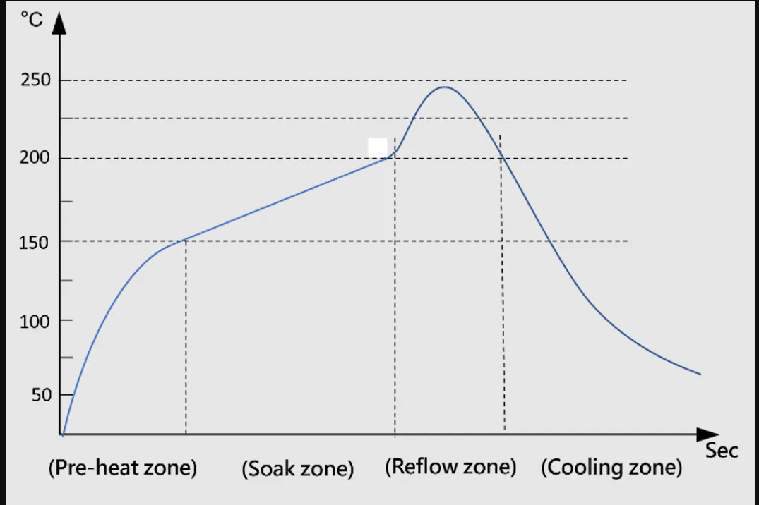
The wave soldering process relies on a delicate balance of temperature, conveyor speed, wave height, and flux application. Even small deviations can cause defects. Here’s how to fine-tune these parameters:
- Solder Bath Temperature: Maintain the solder pot temperature within the recommended range for your alloy, typically 250-260°C for lead-free solders like SAC305. Too low a temperature can cause cold joints, while too high can damage components or cause oxidation.
- Conveyor Speed: Adjust the speed to ensure proper contact time with the solder wave. A speed of 1.0-1.5 meters per minute is often ideal for standard through-hole boards, but test and adjust based on board complexity.
- Wave Height: Set the wave height to just touch the bottom of the PCB without flooding the top side. Excessive height leads to bridging, while too low a height causes skips.
- Preheat Temperature: Ensure the preheat stage brings the board to 100-120°C before soldering to prevent thermal shock and improve solder wetting.
Regularly monitor and calibrate equipment to maintain these settings. Using a thermal profiler to measure board temperatures during the process can help identify inconsistencies.
2. Enhance Flux Application for Better Wetting
Flux plays a vital role in removing oxides and ensuring proper solder wetting. Poor flux application is a leading cause of insufficient solder and cold joints. Consider these tips for wave soldering process optimization:
- Use the correct flux type (e.g., no-clean or water-soluble) based on your board and component requirements.
- Apply flux uniformly using a spray or foam system to avoid dry spots or excess residue.
- Monitor flux density and replenish it regularly to prevent degradation, which can reduce effectiveness.
A well-maintained fluxing system can reduce defects by up to 30%, based on industry case studies, significantly boosting FPY.
3. Improve PCB Design and Layout for Soldering Success
Defects like solder bridging and skips often stem from PCB design issues. As an engineer, collaborating with the design team can prevent problems before they reach the production line. Focus on:
- Component Spacing: Ensure adequate spacing between through-hole leads to avoid bridging. A minimum of 2.5mm between leads is often recommended for wave soldering.
- Pad Size and Shape: Use appropriately sized pads to ensure proper solder flow without excess buildup.
- Orientation: Orient components perpendicular to the direction of the wave to minimize shadowing effects, where trailing leads block solder from reaching others.
Implementing design-for-manufacturability (DFM) guidelines tailored for wave soldering can improve FPY by reducing inherent design-related defects.
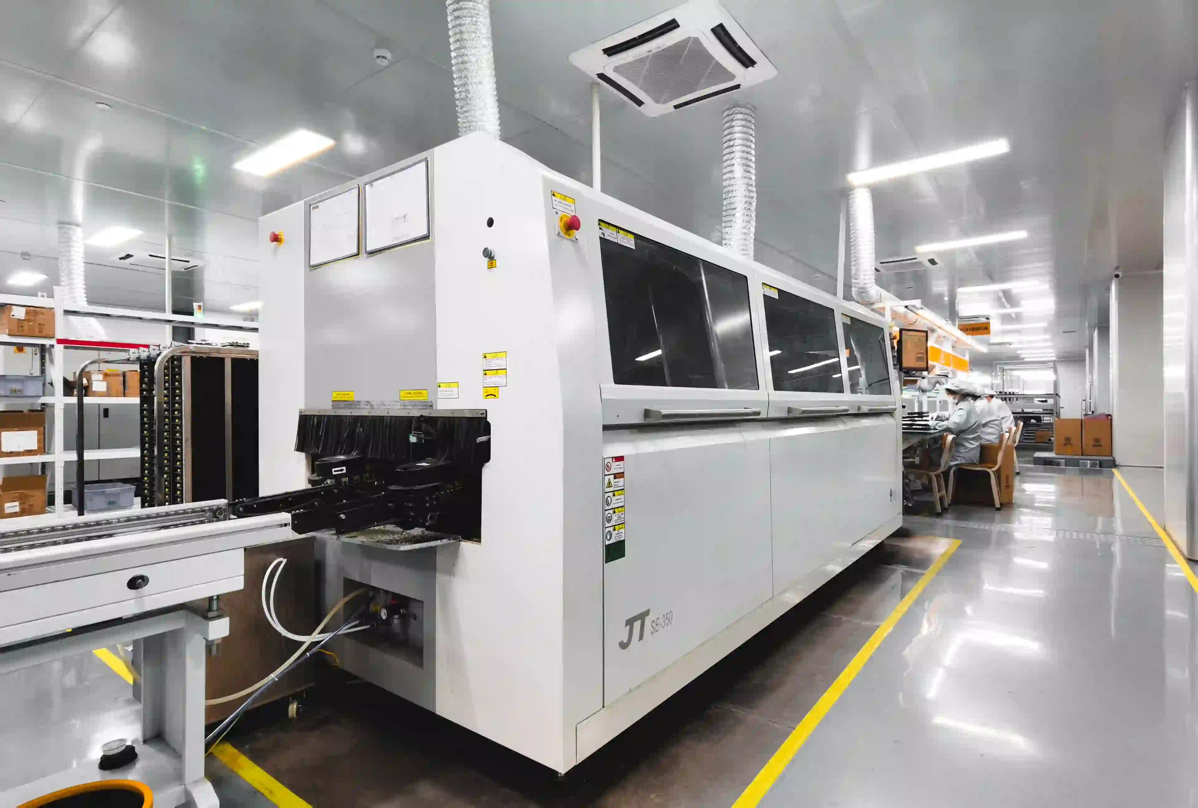
Wave Soldering Defect Reduction Through Equipment Maintenance
Equipment issues are a hidden cause of defects that many overlook. A poorly maintained wave soldering machine can introduce variability that tanks your FPY. Here’s how to keep your equipment in top shape:
- Clean the Solder Pot: Remove dross (oxidized solder) daily to prevent contamination that causes poor wetting. Dross buildup can reduce solder quality and lead to defects.
- Check Wave Uniformity: Inspect the wave for unevenness or turbulence, which can cause inconsistent soldering. Adjust the pump or baffles as needed.
- Calibrate Sensors: Regularly calibrate temperature and speed sensors to ensure accurate readings. A deviation of just 5°C can impact solder joint quality.
Schedule preventive maintenance weekly or based on production volume to avoid unexpected downtime and maintain consistent performance.

Implementing Wave Soldering Quality Control Measures
Quality control is the backbone of sustaining high FPY. Without proper inspection and feedback loops, defects can go unnoticed until they cause major issues. Here are key wave soldering quality control practices:
1. Conduct In-Process Inspections
Perform visual and automated inspections during production to catch defects early. Use magnifying tools or automated optical inspection (AOI) systems to check for bridging, insufficient solder, and other issues. Catching a defect mid-process prevents it from reaching final assembly, saving time and resources.
2. Use Statistical Process Control (SPC)
Implement SPC to monitor key process variables like temperature, speed, and defect rates. By plotting data on control charts, you can spot trends or deviations before they lead to failures. For example, if solder temperature fluctuates beyond ±3°C of the target, it’s a sign to investigate and correct the issue.
3. Test Solder Joint Reliability
Periodically perform destructive testing or cross-section analysis on sample boards to evaluate solder joint integrity. This helps identify hidden issues like voids or cracks that aren’t visible during standard inspections.
By integrating these quality control measures, you can achieve a defect rate below 1%, a benchmark for world-class manufacturing.
Leveraging Design of Experiments (DOE) for Process Optimization
For engineers seeking advanced wave soldering process optimization, Design of Experiments (DOE) is a powerful tool. DOE allows you to systematically test multiple process variables to find the optimal settings for minimizing defects. For instance, you can vary solder temperature, conveyor speed, and flux type across several runs to determine the combination that yields the highest FPY.
A 2006 study on wave soldering quality improvement using DOE found that optimizing key parameters reduced defect rates by over 40% in a high-volume PCB assembly line. While DOE requires time and resources, the long-term gains in FPY and cost savings are significant.
Training and Operator Skill Development
Even the best equipment and processes can fail if operators lack proper training. Human error, such as incorrect machine setup or poor handling of boards, can introduce defects. Invest in regular training programs to ensure operators understand:
- Correct machine operation and parameter settings.
- Proper handling of PCBs to avoid contamination.
- Basic troubleshooting to address minor issues on the spot.
A skilled workforce can improve FPY by reducing variability caused by operator mistakes, making training a worthwhile investment.
Case Study: Real-World FPY Improvement in Wave Soldering
Consider a mid-sized electronics manufacturer struggling with an FPY of 85% in their wave soldering line due to frequent solder bridging and insufficient solder defects. By implementing the strategies above, they achieved remarkable results:
- Adjusted solder bath temperature to a stable 255°C and conveyor speed to 1.2 m/min, reducing cold joints by 25%.
- Upgraded flux application to a precision spray system, cutting insufficient solder defects by 30%.
- Introduced weekly equipment maintenance and daily dross removal, improving overall process consistency.
- Used SPC to monitor defect trends, identifying a recurring wave height issue that was fixed to eliminate bridging.
Within three months, their FPY rose to 96%, saving thousands in rework costs and boosting production capacity. This example shows how a systematic approach to wave soldering defect reduction can yield measurable results.
Conclusion: Building a High-Yield Wave Soldering Process
Maximizing first pass yield in wave soldering is within reach for any electrical engineer willing to focus on process optimization, defect reduction, and quality control. By fine-tuning parameters like temperature and speed, maintaining equipment, improving PCB design, and leveraging tools like DOE and SPC, you can significantly reduce rework and waste. Start with small, measurable changes—such as calibrating your wave soldering machine or training operators—and build toward a comprehensive strategy for continuous improvement.


