 ALLPCB


If you're looking to understand SMT assembly for microelectronics, you're in the right place. Surface Mount Technology (SMT) is a critical process in modern electronics manufacturing, especially for creating compact, high-performance microelectronics. This guide will walk you through the essentials of surface mount technology in microelectronics, covering the SMT process, common defects, and the best equipment to use. Whether you're an engineer, designer, or manufacturer, you'll find practical insights to improve your projects.
In the following sections, we dive deep into the SMT process for microelectronics, explore challenges like defects, and recommend equipment to ensure precision and efficiency. Let's get started on mastering SMT assembly for your next microelectronics project.
What is SMT Assembly in Microelectronics?
SMT assembly for microelectronics refers to the process of mounting electronic components directly onto the surface of a printed circuit board (PCB) without inserting leads through holes. This method is the backbone of modern electronics, especially for microelectronics, where small size and high performance are essential. Unlike traditional through-hole technology, SMT allows for smaller components, tighter layouts, and automated production, making it ideal for devices like smartphones, wearables, and medical equipment.
In microelectronics, SMT is used to create circuits with components as small as 0.4mm x 0.2mm (0402 package size). This miniaturization enables high-density designs, packing thousands of components onto a single board. The result? Faster signal speeds—often exceeding 1 GHz in high-frequency applications—and reduced power consumption, critical for battery-powered devices.
The SMT Process for Microelectronics: Step by Step
The SMT process in microelectronics is a precise, multi-step procedure that ensures components are placed and soldered accurately on a PCB. Here's a detailed breakdown of the process:
1. Solder Paste Application
The process begins with applying solder paste—a mix of tiny solder particles and flux—onto the PCB's pads using a stencil. This paste acts as the adhesive and conductive medium for components. In microelectronics, stencil thickness is often as low as 0.1mm to control paste volume for tiny pads.
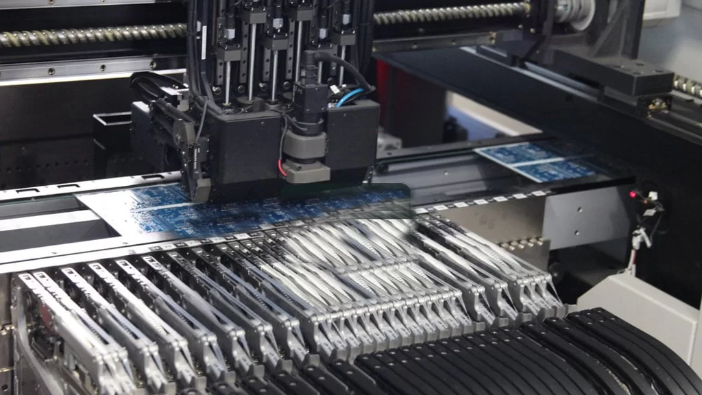
2. Component Placement
Next, automated pick-and-place machines position components onto the solder paste. These machines can place up to 100,000 components per hour with an accuracy of ±0.01mm, crucial for the small-scale needs of microelectronics.
3. Reflow Soldering
Once components are placed, the PCB passes through a reflow oven. The oven heats the board to around 250°C, melting the solder paste to form permanent electrical connections. For microelectronics, precise temperature profiles prevent damage to heat-sensitive components.
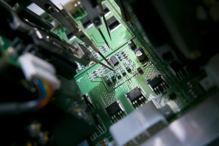
4. Inspection and Testing
After soldering, the board undergoes inspection using Automated Optical Inspection (AOI) systems to detect misplacements or defects. Electrical testing ensures functionality, often measuring impedance values as low as 50 ohms for high-speed circuits.
Advantages of Surface Mount Technology in Microelectronics
Surface mount technology for microelectronics offers several benefits that make it the preferred choice for compact, high-performance devices:
- Miniaturization: SMT components are up to 10 times smaller than through-hole parts, enabling designs with higher component density.
- Faster Production: Automation in SMT reduces assembly time by up to 50% compared to manual through-hole methods.
- Improved Performance: Shorter lead lengths in SMT reduce signal delay, supporting frequencies above 1 GHz for applications like 5G devices.
- Cost Efficiency: Automated processes lower labor costs, and smaller boards reduce material expenses by up to 30%.
These advantages make SMT indispensable for industries like consumer electronics, automotive, and aerospace, where size, speed, and reliability are non-negotiable.
Common SMT Defects in Microelectronics and How to Avoid Them
Despite its precision, SMT defects in microelectronics can occur, leading to costly rework or product failures. Here are the most common issues and solutions to address them:
1. Tombstoning
Tombstoning happens when a small component stands upright on one end due to uneven soldering. This is common with tiny resistors or capacitors in microelectronics (e.g., 0201 packages). To prevent it, ensure balanced pad design and uniform solder paste application. Reflow profiles should also maintain a gradual temperature rise, avoiding rapid heating above 3°C per second.
2. Solder Bridges
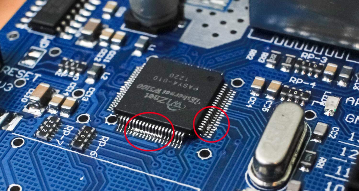
Solder bridges occur when excess solder connects adjacent pads, causing short circuits. In microelectronics, where pad spacing can be as tight as 0.2mm, this is a frequent issue. Use precise stencil designs and reduce solder paste volume by 10-15% for fine-pitch components to avoid this defect.
3. Component Misalignment
Misaligned components can lead to poor connections or non-functional boards. This often results from inaccurate pick-and-place settings. Regular calibration of placement machines to maintain accuracy within ±0.01mm is essential for microelectronics.
4. Cold Solder Joints
Cold solder joints appear dull and grainy, indicating poor bonding due to insufficient heat during reflow. This defect compromises reliability in high-frequency circuits. Optimize reflow oven settings to ensure peak temperatures reach 235-250°C for at least 30 seconds.
Choosing the Right SMT Equipment for Microelectronics
Selecting the best SMT equipment for microelectronics is critical for achieving high precision and efficiency. Here's what to consider when equipping your production line:
1. Pick-and-Place Machines
For microelectronics, choose machines with high-speed placement capabilities (over 50,000 components per hour) and vision systems for accuracy down to 0.01mm. Look for models that support ultra-small components like 01005 packages (0.4mm x 0.2mm).
2. Reflow Ovens
Reflow ovens for microelectronics should offer precise temperature control within ±1°C and multiple heating zones (at least 8-10 zones) to create tailored thermal profiles. This prevents thermal shock to delicate components.
3. Solder Paste Printers
Automated solder paste printers with stencil alignment accuracy of ±0.025mm are essential for fine-pitch applications in microelectronics. They ensure consistent paste deposition on pads as small as 0.3mm wide.
4. Inspection Systems
Advanced AOI systems with high-resolution cameras (at least 5 megapixels) can detect defects on components smaller than 0.5mm. Combining AOI with X-ray inspection helps identify hidden issues like voids in solder joints under BGA (Ball Grid Array) components.
Investing in high-quality equipment tailored for microelectronics can reduce defect rates by up to 40% and improve overall production yield.
Best Practices for Successful SMT Assembly in Microelectronics
To master SMT assembly in microelectronics, follow these best practices to ensure quality and efficiency:
- Design for Manufacturability (DFM): Optimize PCB layouts with adequate spacing (at least 0.2mm between pads) to prevent soldering issues. Use design software to simulate signal integrity at frequencies up to 2 GHz.
- Material Selection: Choose high-quality solder paste with fine particle sizes (Type 4 or 5) for microelectronics to ensure precise application on small pads.
- Environment Control: Maintain a cleanroom environment with humidity levels between 40-60% and temperature around 22°C to prevent contamination or static damage to tiny components.
- Regular Maintenance: Schedule weekly calibration of SMT equipment to maintain placement and soldering accuracy within specified tolerances.
Implementing these practices can boost first-pass yield rates to above 95%, saving time and reducing waste in production.
Future Trends in SMT for Microelectronics
The field of surface mount technology in microelectronics is evolving rapidly, driven by demands for even smaller, faster, and smarter devices. Here are key trends to watch:
- Miniaturization Continues: Components are shrinking further, with 01005 packages becoming standard and even smaller 008004 sizes (0.25mm x 0.125mm) emerging for wearables and IoT devices.
- Advanced Materials: Lead-free solders and low-temperature soldering techniques are gaining traction to meet environmental regulations and protect heat-sensitive components.
- Smart Manufacturing: Integration of IoT and data analytics into SMT equipment allows real-time monitoring, reducing defect rates by predicting maintenance needs before failures occur.
Staying ahead of these trends ensures your SMT processes remain competitive in the fast-paced world of microelectronics.
Conclusion: Elevate Your Microelectronics with SMT Mastery
Mastering SMT assembly for microelectronics is a game-changer for creating cutting-edge, reliable, and compact electronic devices. By understanding the SMT process for microelectronics, addressing common SMT defects in microelectronics, and investing in the right SMT equipment for microelectronics, you can achieve superior results in your projects. The benefits of surface mount technology in microelectronics—from miniaturization to cost efficiency—make it an essential skill for any engineer or manufacturer.
With the insights and best practices shared in this guide, you're well-equipped to tackle the challenges of SMT assembly and push the boundaries of innovation in microelectronics. Start applying these strategies today to build smaller, faster, and more efficient devices that meet the demands of tomorrow's technology.


