ALLPCB


When it comes to PCB assembly for medical devices like CT scanners, reliability isn’t just important—it’s critical. These devices operate in high-stakes environments where a single failure can impact patient safety and diagnostic accuracy. So, how do you ensure high reliability in CT scanner PCB assembly? The answer lies in adopting best practices such as precise surface mount technology (SMT), rigorous automated optical inspection (AOI), thorough X-ray inspection, and a focus on solder joint reliability. In this blog, we’ll dive deep into these practices, offering actionable insights to help engineers and manufacturers build dependable PCBs for medical applications.
Why High Reliability Matters in CT Scanner PCB Assembly
CT scanners are complex medical devices that rely on PCBs to control critical functions, from signal processing to power management. A malfunctioning PCB can lead to inaccurate imaging, delayed diagnoses, or even equipment downtime. For medical device manufacturers, ensuring reliability means adhering to strict standards like ISO 13485 and implementing robust assembly and testing processes. High reliability also reduces the risk of costly recalls and enhances trust in the equipment. With this in mind, let’s explore the best practices for achieving top-tier reliability in PCB assembly for medical devices.
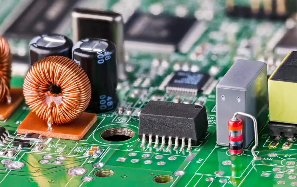
1. Leveraging Surface Mount Technology (SMT) for Precision
Surface mount technology (SMT) is the backbone of modern PCB assembly, especially for compact and high-density designs like those in CT scanners. SMT allows components to be mounted directly onto the PCB surface, reducing size and improving performance. However, precision is key to reliability. Here are some best practices for SMT in medical device PCB assembly:
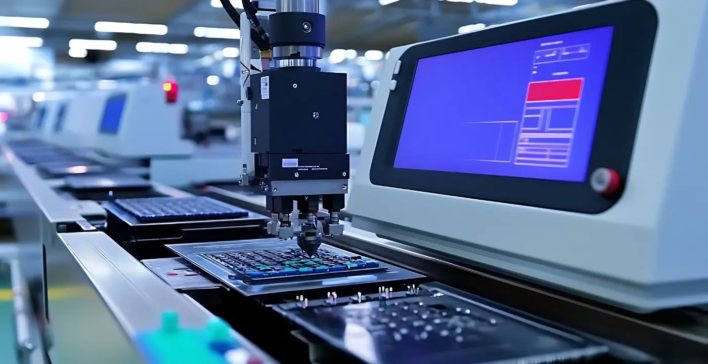
- Use High-Precision Pick-and-Place Machines: Automated machines with placement accuracy of ±0.01 mm ensure components are positioned correctly, minimizing misalignment risks.
- Optimize Stencil Design: Stencil apertures should match component pad sizes to ensure even solder paste application. For example, a 1:1 ratio for aperture-to-pad size often works best for fine-pitch components like 0.5 mm QFN packages.
- Control Reflow Soldering Profiles: Maintain a reflow temperature profile with a peak of 245°C for lead-free solder to prevent thermal stress on components, which can cause cracks or failures.
By focusing on precision during SMT, manufacturers can avoid issues like tombstoning or insufficient soldering, which are critical for the high-density boards used in CT scanners.
2. Implementing Automated Optical Inspection (AOI) for Quality Assurance
Even the most precise assembly process can have flaws, which is why automated optical inspection (AOI) is a must for CT scanner PCB assembly. AOI uses high-resolution cameras and advanced algorithms to detect defects like misaligned components, missing parts, or incorrect polarity. Here’s how to maximize AOI effectiveness:
- Set Up Comprehensive Inspection Points: Inspect after SMT placement and post-reflow soldering to catch issues early. AOI systems can detect defects as small as 0.1 mm, ensuring no detail is missed.
- Customize Inspection Parameters: Adjust AOI settings for the specific components used in CT scanner PCBs, such as high-density BGA chips, to reduce false positives and improve accuracy.
- Integrate with Real-Time Feedback: Use AOI data to adjust assembly processes instantly, preventing recurring defects and maintaining consistent quality.
AOI is a non-destructive and efficient way to ensure quality, making it indispensable for PCB assembly for medical devices where zero-defect standards are the goal.
3. Using X-Ray Inspection for Hidden Defect Detection
While AOI excels at surface-level inspection, it can’t see beneath components or inside solder joints. This is where X-ray inspection comes in, especially for complex CT scanner PCBs with ball grid array (BGA) components or multilayer boards. X-ray systems penetrate materials to reveal hidden issues like voids, cracks, or insufficient solder. Here’s how to implement effective X-ray inspection:
- Focus on High-Risk Areas: Prioritize inspection of BGA and QFN components, where solder joints are hidden under the package. X-ray systems with resolutions down to 1 μm can detect micro-voids that impact reliability.
- Use 3D X-Ray for Multilayer Boards: CT scanner PCBs often have 8 or more layers. 3D X-ray imaging helps identify defects in inner layers, such as misaligned vias or delamination.
- Adhere to Safety Standards: Ensure X-ray equipment complies with radiation safety guidelines to protect operators while maintaining thorough inspections.
X-ray inspection is a powerful tool for ensuring the integrity of hidden connections, a critical factor in achieving high reliability for medical device PCBs.
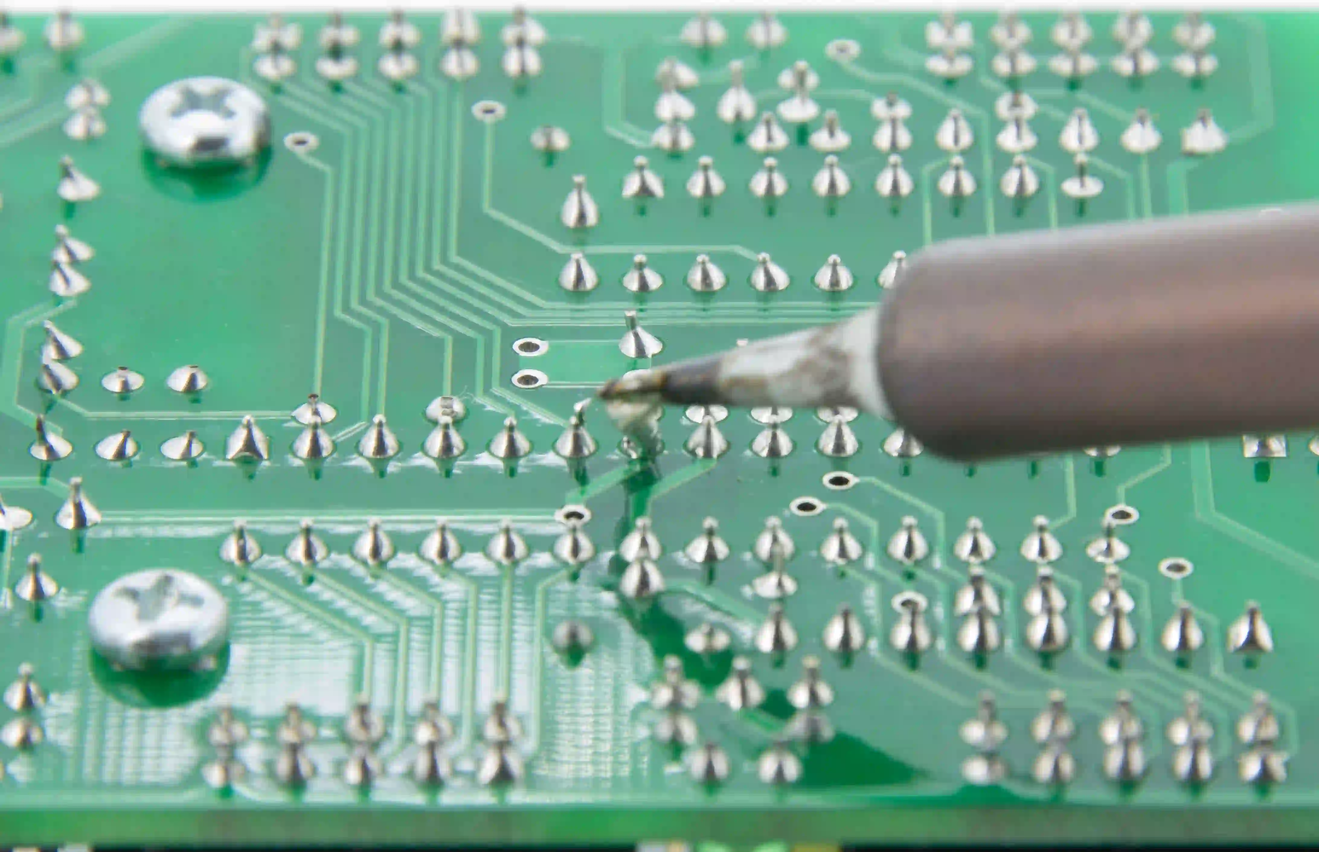
4. Ensuring Solder Joint Reliability for Long-Term Performance
Solder joint reliability is at the heart of PCB durability, especially in CT scanners where thermal cycling, vibration, and constant operation can stress connections. Poor solder joints can lead to intermittent failures or complete breakdowns. Follow these best practices to ensure robust solder joints:
- Choose the Right Solder Alloy: Use lead-free solder alloys like SAC305 (Sn96.5Ag3.0Cu0.5) for its excellent thermal fatigue resistance and compliance with RoHS standards.
- Control Solder Paste Volume: Apply precise amounts of solder paste to avoid insufficient or excessive solder, which can cause weak joints or bridging. For fine-pitch components, aim for a paste thickness of 0.1 mm to 0.15 mm.
- Perform Thermal Cycling Tests: Test PCBs under temperature ranges of -40°C to 85°C for 1000 cycles to simulate real-world conditions and identify potential solder joint failures early.
- Monitor Intermetallic Compound (IMC) Growth: Excessive IMC growth at solder joints can weaken connections over time. Use cross-sectional analysis during testing to ensure IMC thickness stays below 3 μm after accelerated aging tests.
Reliable solder joints are non-negotiable for CT scanner PCBs, as they directly impact the device’s ability to function consistently over years of use.
5. Additional Best Practices for High Reliability in Medical PCB Assembly
Beyond the core techniques, several other practices contribute to high reliability in PCB assembly for medical devices. These include:
- Material Selection: Use high-quality laminates like FR-4 with a glass transition temperature (Tg) of at least 170°C to withstand the thermal demands of CT scanner operation.
- Design for Manufacturability (DFM): Optimize PCB layouts to minimize signal interference, with controlled impedance traces (e.g., 50 ohms for high-speed signals) to ensure accurate data transmission in imaging systems.
- Environmental Testing: Subject assembled PCBs to humidity (85% RH at 85°C) and vibration tests (10-500 Hz at 5G) to confirm durability in hospital environments.
- Traceability and Documentation: Maintain detailed records of every assembly step, including component batch numbers and test results, to comply with medical regulations and enable quick root-cause analysis if issues arise.
These practices, combined with the core techniques of SMT, AOI, and X-ray inspection, create a comprehensive approach to reliability.
6. The Role of Standards and Compliance in Medical PCB Assembly
Compliance with industry standards is non-negotiable for CT scanner PCB assembly. Standards like IPC-A-610 (Acceptability of Electronic Assemblies) and ISO 13485 (Quality Management for Medical Devices) provide guidelines for quality and reliability. For instance, IPC-A-610 Class 3 standards, which apply to high-reliability electronics like medical devices, require zero visible defects in solder joints and strict adherence to assembly tolerances. Regular audits and certifications ensure that every step of the assembly process meets these stringent requirements, protecting both manufacturers and end-users.
Conclusion: Building Trust Through Reliable CT Scanner PCB Assembly
Achieving high reliability in CT scanner PCB assembly requires a multi-faceted approach, from leveraging surface mount technology (SMT) for precision to using automated optical inspection (AOI) and X-ray inspection for quality control, and prioritizing solder joint reliability for durability. By following the best practices outlined in this blog, manufacturers can produce PCBs that meet the demanding requirements of PCB assembly for medical devices. At ALLPCB, we’re committed to supporting engineers and manufacturers with the tools and expertise needed to build reliable, high-performance PCBs for critical applications like CT scanners. Let’s work together to ensure patient safety and diagnostic accuracy through top-tier assembly practices.