 ALLPCB


Are you looking to ensure the quality of your printed circuit boards (PCBs) before assembling components? Bare board testing is a critical step in PCB manufacturing that helps identify defects and ensures reliability. In this comprehensive guide, we’ll explore bare board testing methods, electrical testing for bare PCBs, and specific techniques like flying probe testing and bed-of-nails testing. We’ll also cover how these processes ensure continuity and isolation, helping you achieve flawless performance in your final product.
What Is Bare Board Testing and Why Is It Important?
Bare board testing refers to the process of inspecting a PCB before any electronic components are mounted on it. At this stage, the board is just a “bare” structure of conductive traces, pads, and vias. Testing at this point helps catch manufacturing defects like short circuits, open circuits, or incorrect trace widths that could lead to failures after assembly.
The importance of bare board testing cannot be overstated. Identifying issues early saves time and money, as assembling components on a faulty board can result in costly rework or scrapped products. For instance, a short circuit on a bare PCB could damage expensive components if not detected before assembly. By conducting thorough testing, manufacturers can ensure the board meets design specifications and industry standards, ultimately leading to higher reliability in the final product.
Key Bare Board Testing Methods for Reliable PCBs
There are several bare board testing methods used in the industry to verify the integrity of PCBs. Each method has its unique advantages, depending on the complexity of the board and production volume. Below, we dive into the most common techniques, focusing on electrical testing for bare PCBs.
1. Visual Inspection: The First Line of Defense
Before electrical testing begins, a simple visual inspection is often performed. This step involves checking the bare PCB for physical defects like scratches, misaligned layers, or incomplete etching. While this method doesn’t test electrical performance, it can catch obvious issues that might affect later testing or assembly.
Visual inspection is often aided by automated optical inspection (AOI) systems, which use cameras and software to detect surface-level flaws with high precision. For example, AOI can identify trace widths that deviate from the design by as little as 0.1 mm, ensuring the board meets tight tolerances.
2. Electrical Testing for Bare PCBs: Ensuring Functionality
Electrical testing for bare PCBs is the core of bare board testing. This process verifies that the conductive paths on the board are intact and free from defects. It focuses on two critical aspects: continuity and isolation.
- Continuity Testing: Ensures that electrical paths (traces and vias) are connected as per the design. A break in continuity, or an “open,” means the current cannot flow through a path, rendering the board unusable for certain functions.
- Isolation Testing: Confirms that there are no unintended connections (shorts) between separate conductive paths. A short circuit can cause catastrophic failures, especially in high-voltage applications.
Electrical testing typically uses specialized equipment to apply test signals and measure parameters like resistance. For instance, a typical test might check if the resistance between two isolated nets is above 10 megaohms, confirming proper insulation.
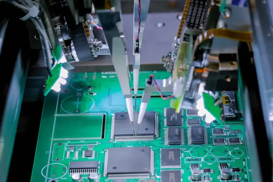
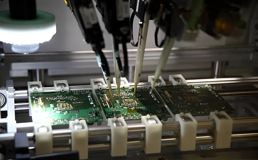
3. Flying Probe Testing for Bare Boards: Precision and Flexibility
Flying probe testing for bare boards is a highly versatile and precise method of electrical testing. This technique uses robotic probes that move across the board to make contact with test points, measuring continuity and isolation without the need for a custom fixture.
The main advantage of flying probe testing is its flexibility. It’s ideal for low-volume production or prototypes because it doesn’t require a dedicated test fixture, which can be expensive and time-consuming to design. Modern flying probe systems can test boards with a pad pitch as small as 0.2 mm, making them suitable for high-density designs.
However, flying probe testing is slower than other methods due to the sequential nature of probe movements. For a complex board with thousands of test points, testing might take several minutes, which can be a bottleneck in high-volume manufacturing.
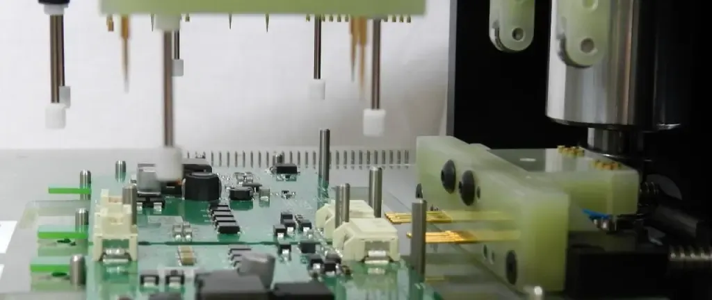
4. Bed-of-Nails Testing for Bare Boards: Speed for High-Volume Production
Bed-of-nails testing for bare boards is a faster alternative to flying probe testing, commonly used in high-volume production. This method uses a custom fixture with an array of spring-loaded pins (the “nails”) that align with test points on the PCB. When the board is pressed onto the fixture, the pins make contact with the test points simultaneously, allowing for rapid electrical testing.
The speed of bed-of-nails testing makes it ideal for mass production. For example, a bed-of-nails fixture can test a board with 5,000 test points in under 10 seconds, compared to several minutes for flying probe testing. However, creating a custom fixture for each board design can cost thousands of dollars and take weeks, making this method less practical for small runs or frequent design changes.
Ensuring Continuity and Isolation in PCB Manufacturing
Ensuring continuity and isolation is the cornerstone of bare board testing. Without proper continuity, signals cannot travel through the board as intended, leading to functional failures. Without isolation, unintended shorts can cause current leakage, overheating, or even fires in extreme cases.
To ensure continuity, testers apply a low-voltage signal to one end of a conductive path and measure if it reaches the other end. A resistance value close to 0 ohms indicates a good connection, while a high resistance or infinite value signals an open circuit. For isolation, testers measure the resistance between two separate nets. A value of 10 megaohms or higher typically confirms that the nets are properly insulated.
In high-frequency applications, additional tests like impedance testing may be conducted to ensure signal integrity. For example, a PCB designed for a 5G application might require controlled impedance traces with a tolerance of ±10% around a target value of 50 ohms. Failing to meet these specs can degrade signal performance, leading to data loss or interference.
Benefits of Bare Board Testing Before Component Assembly
Conducting bare board testing before component assembly offers several key benefits:
- Cost Savings: Fixing a defect on a bare board is far cheaper than repairing an assembled board. Reworking a fully populated PCB can cost 10 times more due to the labor and risk of damaging components.
- Improved Reliability: Early detection of faults ensures that only high-quality boards move to the assembly stage, reducing the risk of failures in the field.
- Faster Production: Identifying and resolving issues early prevents delays during assembly or final testing, keeping production schedules on track.
- Compliance with Standards: Bare board testing ensures that PCBs meet industry standards like IPC-6012 for rigid boards, which specify acceptable defect levels and performance criteria.
Challenges in Bare Board Testing and How to Overcome Them
While bare board testing is essential, it comes with certain challenges. Understanding these hurdles and how to address them can improve the testing process.
- Complex Designs: High-density boards with fine-pitch components can be difficult to test due to limited access to test points. Using flying probe testing or advanced fixtures can help overcome this issue.
- Cost of Fixtures: Bed-of-nails testing requires expensive custom fixtures. For small runs, opting for flying probe testing can be more cost-effective.
- Time Constraints: Thorough testing can slow down production. Balancing speed and quality by prioritizing critical test points or using automated systems can help manage time constraints.
How to Choose the Right Bare Board Testing Method
Selecting the appropriate bare board testing method depends on several factors, including production volume, board complexity, and budget. Here’s a quick guide to help you decide:
- Low-Volume or Prototypes: Choose flying probe testing for its flexibility and lack of fixture costs. It’s ideal for testing a few boards or designs that are still in development.
- High-Volume Production: Opt for bed-of-nails testing to maximize speed and efficiency. The upfront cost of the fixture is offset by the time saved in large-scale manufacturing.
- High-Density Boards: Use advanced flying probe systems or hybrid approaches that combine multiple testing methods to ensure coverage of all test points.
Additionally, consider the specific requirements of your application. For example, if your PCB will operate at high frequencies, ensure that impedance testing is included in the process to verify signal integrity.
Conclusion: Building Quality into Every PCB with Bare Board Testing
Bare board testing is a vital step in PCB manufacturing that ensures quality before component assembly. By employing effective bare board testing methods like electrical testing for bare PCBs, flying probe testing, and bed-of-nails testing, manufacturers can catch defects early, save costs, and improve reliability. Ensuring continuity and isolation through these techniques guarantees that the board will perform as intended, even in demanding applications.
At ALLPCB, we are committed to delivering high-quality PCBs through rigorous testing and advanced manufacturing processes. Whether you’re working on a prototype or a large production run, understanding and implementing the right testing methods can make all the difference in achieving a flawless final product.


