ALLPCB


If you're looking for practical guidance on mounting LCC (Leadless Chip Carrier) magnetic sensors, particularly following the AN-216 guidelines from Honeywell Aerospace, you've come to the right place. This blog post dives deep into the best practices for PCB design, SMT (Surface Mount Technology) rules, solder mask usage, solder reflow processes, and circuit board pad design to ensure optimal performance of these sensors. Whether you're an electronics engineer or a PCB designer, you'll find actionable tips to help you avoid common pitfalls and achieve reliable results.
Below, we’ll explore the critical aspects of mounting LCC magnetic sensors, breaking down each step with detailed explanations and practical advice. Let’s get started with the essentials of PCB design and assembly for these specialized components.
Understanding LCC Magnetic Sensors and AN-216 Guidelines
LCC magnetic sensors are compact, high-performance components often used in aerospace, automotive, and industrial applications to detect magnetic fields with precision. These sensors come in a leadless chip carrier package, which means they require specific mounting techniques to ensure proper electrical and mechanical connections on a printed circuit board (PCB). The AN-216 application note from Honeywell Aerospace provides detailed recommendations for mounting these sensors to avoid damage and ensure accurate performance.
The key to successful mounting lies in adhering to strict PCB design guidelines, following SMT PCB rules, and paying close attention to solder mask usage and reflow processes. By understanding the unique requirements of LCC packages, such as their small size and lack of leads, you can prevent issues like misalignment, poor solder joints, or thermal stress during assembly.
Why Proper Mounting Matters for LCC Magnetic Sensors
Improper mounting of LCC magnetic sensors can lead to a range of problems, including signal inaccuracies, mechanical failure, or even complete sensor malfunction. These sensors are often used in critical applications where reliability is non-negotiable. Following the AN-216 guidelines helps ensure that the sensor operates within its specified parameters, such as maintaining sensitivity to magnetic fields (often measured in gauss or tesla) and avoiding interference from nearby components.
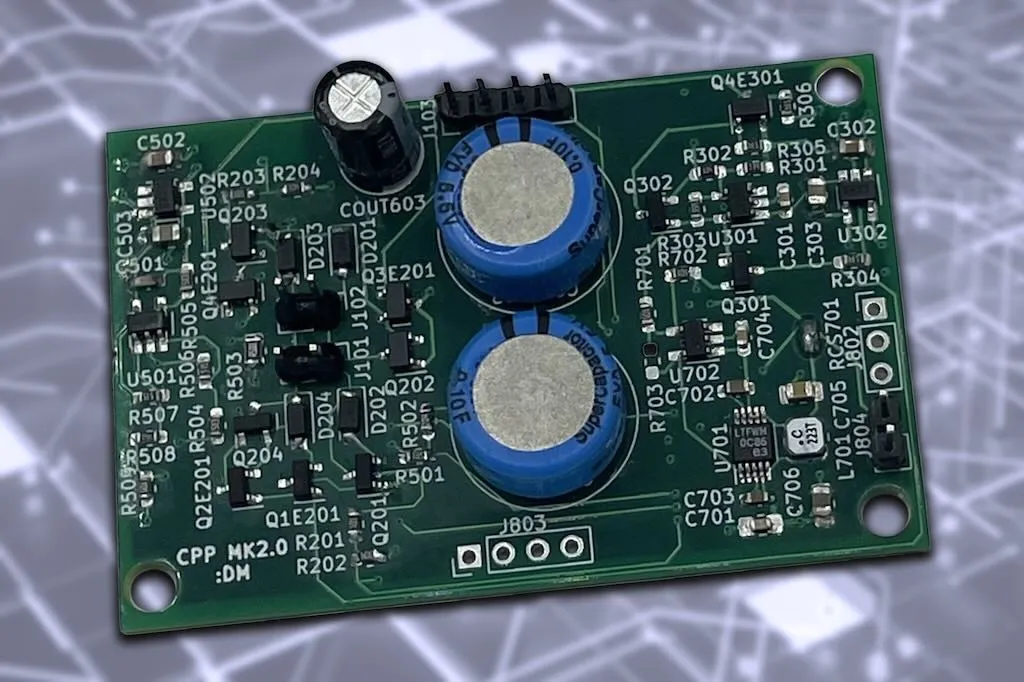
PCB Design Guidelines for LCC Magnetic Sensors
Designing a PCB for LCC magnetic sensors starts with a solid understanding of layout requirements. The AN-216 note emphasizes the importance of minimizing stress on the sensor package and ensuring proper alignment during assembly. Here are the key PCB design guidelines to follow:
- Pad Layout and Dimensions: Ensure that the pad layout matches the sensor’s footprint as specified in the datasheet. For most LCC packages, pads should be designed with a 1:1 ratio to the sensor’s contact area, typically ranging from 0.5 mm to 1.0 mm in width, depending on the package size. This prevents solder bridging and ensures a strong connection.
- Clearance and Spacing: Maintain adequate clearance around the sensor to avoid interference from other components. A minimum spacing of 2 mm from other components is often recommended to reduce electromagnetic interference (EMI), which can affect sensor readings.
- Trace Routing: Keep signal traces short and direct to minimize noise. For high-sensitivity magnetic sensors, avoid routing high-current traces near the sensor, as they can introduce unwanted magnetic fields that interfere with readings (e.g., currents above 100 mA can create measurable disturbances).
By focusing on these PCB design guidelines, you create a foundation for reliable sensor performance. A well-designed layout not only supports accurate mounting but also enhances the overall functionality of the circuit board.
SMT PCB Rules for Mounting LCC Sensors
Surface Mount Technology (SMT) rules are critical when dealing with LCC packages due to their small size and lack of leads. The following SMT PCB rules align with the AN-216 recommendations and industry best practices:
- Component Placement Accuracy: Use automated pick-and-place machines with high precision (placement accuracy of ±0.05 mm or better) to ensure the sensor is aligned correctly with the pads. Misalignment by even 0.1 mm can lead to poor solder joints or connection failures.
- Stencil Design: Design the stencil aperture to match the pad size, typically with a 1:1 ratio. This ensures the right amount of solder paste is applied—usually around 0.1 mm to 0.15 mm in thickness—to create a strong bond without excess paste causing shorts.
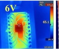
- Avoid Overloading Components: Limit the number of components placed near the sensor during the initial assembly phase to reduce thermal stress. High-density boards can create uneven heat distribution during reflow, potentially damaging the sensor.
Following these SMT PCB rules ensures that the sensor is mounted with precision and reliability, reducing the risk of defects during manufacturing.
Solder Mask Usage for LCC Magnetic Sensors
Solder mask usage plays a vital role in protecting the PCB and ensuring proper soldering of LCC magnetic sensors. The solder mask is a thin layer of polymer applied to the PCB to prevent solder from adhering to unintended areas. Here’s how to optimize solder mask usage for these sensors:
- Define Solder Mask Openings: The solder mask should expose only the pads where the sensor will be mounted. The opening should be slightly larger than the pad (by about 0.05 mm to 0.1 mm on each side) to allow for proper solder flow while preventing bridging between adjacent pads.
- Avoid Mask on Pads: Ensure that no solder mask covers the contact pads, as this can interfere with the solder joint formation. A non-solder mask defined (NSMD) pad design is often recommended for LCC packages to improve reliability.
- Material Selection: Use a high-quality solder mask material that can withstand the temperatures of the reflow process (up to 260°C for lead-free solder). This prevents cracking or peeling, which could expose copper traces and lead to corrosion.
Proper solder mask usage not only protects the PCB but also enhances the durability of the solder joints, ensuring long-term performance of the magnetic sensor.
Solder Reflow Process for Reliable Mounting
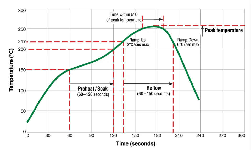
The solder reflow process is a critical step in mounting LCC magnetic sensors. This process involves heating the PCB to melt the solder paste, creating a permanent bond between the sensor and the board. The AN-216 guidelines provide specific recommendations to avoid thermal damage to the sensor. Here’s how to optimize the solder reflow process:
- Temperature Profile: Follow a controlled temperature profile during reflow. For lead-free solder, the peak temperature should be between 240°C and 260°C, with a time above liquidus (TAL) of 30 to 60 seconds. Avoid exceeding the sensor’s maximum temperature rating, often around 260°C for 10 seconds, to prevent internal damage.
- Preheat Stage: Preheat the PCB gradually (at a rate of 1°C to 3°C per second) to minimize thermal shock. A preheat temperature of 150°C to 180°C for 60 to 120 seconds helps activate the flux in the solder paste and prepares the board for reflow.
- Cooling Rate: After reflow, cool the board at a controlled rate (no more than 6°C per second) to prevent thermal stress on the sensor. Rapid cooling can cause cracks in the solder joints or damage the sensor package.
Monitoring the reflow oven’s temperature profile using a thermal profiler is highly recommended to ensure consistency across multiple boards. A well-executed reflow process results in strong, reliable solder joints that maintain the sensor’s performance over time.
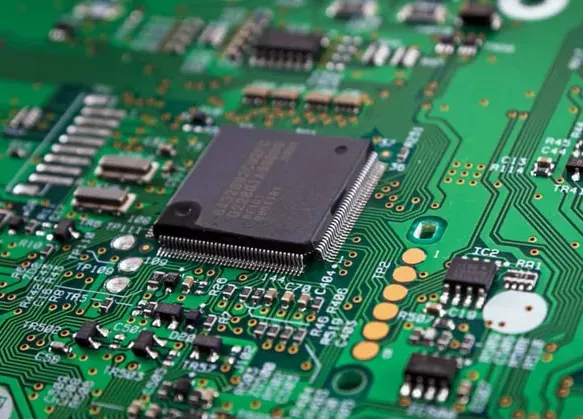
Circuit Board Pads: Design and Preparation Tips
The design and preparation of circuit board pads are crucial for achieving a secure connection with LCC magnetic sensors. Poor pad design can lead to weak solder joints or misalignment during assembly. Follow these tips to optimize your circuit board pads:
- Pad Size and Shape: Match the pad size to the sensor’s contact area, typically ranging from 0.5 mm to 1.0 mm in width for small LCC packages. Use a rectangular or square shape for better solder distribution and alignment.
- Surface Finish: Choose a surface finish that enhances solderability, such as Electroless Nickel Immersion Gold (ENIG) or Hot Air Solder Leveling (HASL). ENIG, for instance, provides a flat surface with excellent corrosion resistance, ensuring a reliable connection.
- Pad Cleanliness: Before assembly, ensure that the pads are free from contaminants like dust or oxidation. Use a cleaning process, such as ultrasonic cleaning or plasma treatment, to prepare the surface for soldering.
Well-designed and prepared circuit board pads are the foundation of a successful mounting process, ensuring that the sensor remains securely attached and performs as expected.
Common Challenges and Solutions in Mounting LCC Magnetic Sensors
Even with the best preparation, challenges can arise when mounting LCC magnetic sensors. Here are some common issues and their solutions:
- Misalignment During Placement: If the sensor shifts during placement, it can lead to poor connections. Solution: Use high-precision pick-and-place equipment and verify alignment with automated optical inspection (AOI) systems after placement.
- Solder Joint Defects: Issues like voids or insufficient solder can weaken the connection. Solution: Optimize stencil design and reflow profile to ensure even solder distribution. X-ray inspection can help detect hidden voids post-assembly.
- Thermal Damage: Excessive heat during reflow can damage the sensor. Solution: Strictly adhere to the recommended temperature profile and avoid rework cycles that expose the sensor to additional heat.
By anticipating these challenges and implementing the suggested solutions, you can minimize risks and ensure a smooth mounting process.
Final Thoughts on Mounting LCC Magnetic Sensors
Mounting LCC magnetic sensors following the AN-216 guidelines from Honeywell Aerospace requires careful attention to PCB design guidelines, SMT PCB rules, solder mask usage, solder reflow processes, and circuit board pad preparation. Each step, from layout design to final assembly, plays a critical role in ensuring the sensor’s reliability and performance in demanding applications.
By following the tips outlined in this blog, you can avoid common pitfalls and achieve consistent, high-quality results. Whether you’re working on aerospace systems or industrial equipment, proper mounting techniques will help you maximize the accuracy and longevity of your magnetic sensors.
At ALLPCB, we’re committed to supporting engineers and designers with resources and services to bring their projects to life. From PCB fabrication to assembly, we’re here to help you navigate the complexities of mounting specialized components like LCC magnetic sensors.