ALLPCB


When reading a MOSFET datasheet, you need to know what you're looking for. Some parameters are obvious (BVDS, RDS(ON), gate charge), others are ambiguous (IDA, SOA curves), and some are of limited practical use (switching times as presented). This article series decodes FET datasheets so designers can identify the parameters that matter for their applications and avoid misleading comparisons between different suppliers.
1 UIS / Avalanche Rating
The Unclamped Inductive Switching (UIS) rating, widely used in MOSFET datasheets since the mid-1980s, is a useful metric. Although repeated avalanche operation is not recommended in real applications, engineers use UIS to screen out devices that are fragile under avalanche stress. Devices that show weak UIS capability or severe degradation over temperature (for example, more than 30% change between 25°C and 125°C) should be avoided because they are more likely to fail.
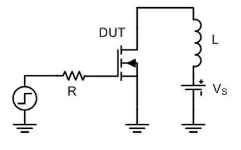
UIS testing uses the circuit shown below. With the FET off, a supply voltage is applied and leakage is checked. While the FET is on, the inductor current is allowed to ramp. When the desired current is reached the FET is turned off; the L·di/dt voltage swing across the MOSFET exceeds its breakdown voltage, activating its intrinsic parasitic bipolar transistor and causing an effective avalanche event. The test is repeated with increasing current until leakage checks fail, indicating device damage.

The equation E = 1/2 L I^2 is used to calculate the device avalanche energy, representing the energy stressed during the test. By changing the inductor value, the stress applied to the device under test can be altered. Larger inductors lower the UIS current that causes failure, but the increased inductance raises the calculated energy, so a lower current can correspond to a higher energy. Table 1 shows data collected from TI's CSD18502KCS 60V NexFET illustrating this relationship.
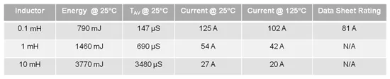
For consistency, some manufacturers use a small inductance (TI uses 0.1 mH) when qualifying production devices and publish the associated energy. Because there is no strict industry standard for the test inductor, some vendors use larger inductors in UIS tests to make their devices appear to have higher avalanche energy capability. Designers should therefore confirm UIS test conditions before comparing avalanche ratings from different suppliers.
2 Safe Operating Area (SOA) Curve
The Safe Operating Area (SOA) curve is one of the most frequently asked-about items for power MOSFETs after current ratings. SOA interpretation requires care because suppliers use different methods to generate SOA data, and the usefulness of SOA data depends on how well the reader understands those methods. Although FETs are useful in linear or hot-plug applications where they operate in their linear region, many users also rely on the SOA curve as an indicator of overall ruggedness and power-handling capability.
An SOA curve can be shaped by five distinct limiting conditions. The SOA example shown in the datasheet for TI's 100V D2PAK CSD19536KTT illustrates this. TI operates a powerful SOA tester capable of applying kilowatts into a FET for pulse durations down to about 100 μs. To generate the datasheet curve, the device is stressed repeatedly at various voltages and pulse durations until failure points are recorded. Each point corresponds to a device forced to fail, and these failure points determine the slope and location of the thermal runaway line.
Because of part-to-part variation, vendors may apply derating to measured thermal-runaway lines when publishing SOA. Some suppliers publish actual failure points and represent them as guaranteed SOA, while others derate measured curves to provide a safety margin. There is no uniform industry standard for this, so without underlying failure data it is difficult to judge relative device ruggedness from SOA curves alone.
The next part of this series will cover the current limits commonly shown on MOSFET datasheet front pages, explain how those values are derived, and discuss their practical relevance for designers.
3 Continuous Current Ratings
Continuous current ratings on MOSFET datasheets are often theoretical rather than measured. Unlike parameters such as RDS(ON) or gate charge, continuous current limits are frequently calculated and can be derived in different ways. One common rating is the package current rating, which depends on the internal bond wires and package materials and is independent of ambient conditions. Exceeding this rating does not cause immediate failure but can reduce device lifetime via mechanisms such as bond-wire fusing, molding compound thermal degradation, and electromigration.
Another common rating is the chip limit, often specified with the case temperature held at 25°C. This assumes an ideal heatsink and uses only the junction-to-case thermal resistance (RθJC) to compute the maximum dissipation (equations shown in the datasheet). In other words, it assumes RθCase-to-Ambient is zero, which is not realistic in most applications; treat this current rating as an indicator of RDS(ON) and thermal impedance behavior rather than an application-ready DC current.
Some QFN datasheets include a third continuous current derived using the measured RθJA (junction-to-ambient). Using RθJA (for example, a typical SON 5x6 package value around 40°C/W) to calculate maximum power assumes the QFN dissipates only a few watts in the application and therefore provides a more realistic DC current rating for QFN parts without heatsinks.
The fourth part of this series will present a similar analysis for pulse current ratings (IDM) and relate IDM to other datasheet parameters, including SOA.
4 Pulse Current Ratings
Pulse current ratings and how they are computed, and how they appear on an FET's SOA, are important to understand. The datasheet pulse current rating (IDM) is similar to the continuous current rating in that it is often a theoretical calculation. IDM is typically calculated as a thermal constraint using a transient thermal impedance (ZθJC for a given pulse duration) and an allowed duty cycle (often specified in an absolute-maximum table).
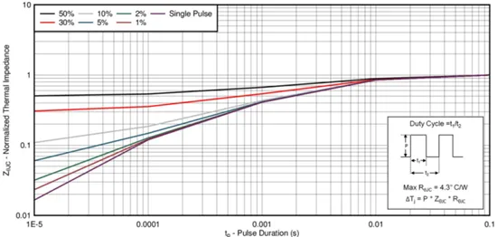
For example, the CSD17579Q5A 30V N-channel MOSFET lists a 105 A maximum pulse current for pulses ≤100 μs and duty cycle ≤1%. To determine the transient thermal impedance for that pulse condition, refer to the standardized Zθ curve. At 100 μs and 1% duty, the normalized factor is about 0.12; multiply this by the DC RθJC (4.3°C/W) to obtain ZθJC ≈ 0.52°C/W. Using that transient thermal impedance to compute maximum power yields a thermal-limited current of about 119 A. However, the datasheet specifies 105 A because, on the SOA plot, the 100 μs line encounters the RDS(ON) limit before the thermal limit, and the intersection occurs at 105 A. In such cases the absolute pulse current is reduced to reflect the device's RDS(ON) limitation.
For each major pulse duration shown on the SOA, the corresponding current limit is calculated (assuming it does not first hit the RDS(ON) limit); this value defines the upper end of those SOA lines. Because the absolute maximum pulse current is a theoretical value, measurements are used where possible to validate capability. In practice, many test setups limit measured pulse currents to about 400 A, which can impose an artificial upper bound on published IDM values. Some vendors similarly cap published IDM, while others do not. Theoretical IDM values can become unrealistically large for parts with very low RDS(ON) and thermal impedance, so designers should consider tested limits and realistic test conditions when comparing datasheets.
The fifth part of this series will provide a similar analysis for IDM and show its relationship to other datasheet parameters including the SOA.
5 Switching Parameters
Finally, some switching-related parameters appearing in MOSFET datasheets deserve scrutiny. Output charge (QOSS) and reverse-recovery charge (Qrr) of the intrinsic diode are key contributors to switching losses in many high-frequency power converters. However, these parameters depend strongly on test conditions. Figure 1 shows Qoss and Qrr measured on TI's CSD18531Q5A at two different di/dt rates. At 360 A/μs, Qrr was measured at 85 nC; at 2000 A/μs, Qrr increased to 146 nC. Because there is no industry-standard di/dt for these measurements, some competitors measure at very low di/dt (for example 100 A/μs) to present lower Qrr figures.
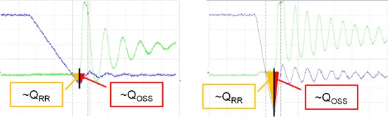
Qrr can be even more dependent on the diode forward current (If). Complicating comparisons further, some vendors include QOSS within the Qrr specification rather than listing it separately. Other factors such as PCB parasitic inductances and measurement methods also make cross-vendor comparison difficult. These parameters are important, but reliable comparison requires measuring devices under consistent or independently controlled conditions.
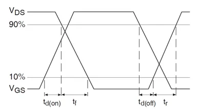
Switching times often listed in datasheets are another set of parameters to treat cautiously. The turn-on and turn-off timing parameters are highly dependent on test circuits and conditions; they mainly reflect driver strength and leakage effects rather than intrinsic device switching speed. Some vendors specify switching times at higher test currents, others at 1 A to make their parts look faster. Gate charge and internal gate resistance (Rg) are generally more indicative of actual switching behavior and are less susceptible to such specmanship.