ALLPCB


Overview
A bipolar junction transistor (BJT), commonly called a transistor, is a semiconductor device used to control current. It can amplify weak signals into larger electrical signals and also serve as a contactless switch. The word semiconductor appears in source references as the device material class, and the term transistor is often used interchangeably in component descriptions.
Structure
A transistor is formed on a single semiconductor substrate by creating two closely spaced PN junctions. The two PN junctions divide the substrate into three regions: the middle region is the base, and the outer regions are the emitter and the collector. The two main arrangements are PNP and NPN.
Materials and Doping
Transistors are typically made from either germanium or silicon. Each material can be configured as either NPN or PNP, with silicon NPN and germanium PNP among the commonly used types. Here, N denotes negative (from "Negative"); an N-type semiconductor is produced by doping high-purity silicon with phosphorus to introduce free electrons that conduct under applied voltage. P denotes positive (from "Positive"); a P-type semiconductor is produced by doping with boron, creating holes that facilitate conduction.
Operation Principle
Electron motion details are omitted here. In practical use, the transistor's current-amplifying action can be understood analogously to a valve: a small input current or voltage at the base controls a larger current between collector and emitter.
Modes of Operation
- Cutoff: When the voltage applied to the emitter junction is below the junction forward voltage, base current is essentially zero, and collector and emitter currents are zero. The transistor loses its current-amplifying function and behaves like an open switch between collector and emitter. This is the cutoff state.
- Active (Amplification): When the emitter junction forward voltage exceeds the junction threshold and is at an appropriate value, the emitter junction is forward biased and the collector junction is reverse biased. In this condition, base current controls collector current, and the transistor provides current amplification. The current gain is β = ΔIc / ΔIb. This is the active, or amplifying, state.
- Saturation: If the emitter junction is forward biased and base current increases beyond a certain point, collector current no longer increases proportionally and instead approaches a near-constant value. The transistor loses its current-amplifying behavior, the voltage between collector and emitter becomes very small, and the device behaves like a closed switch between collector and emitter. This is the saturation state.
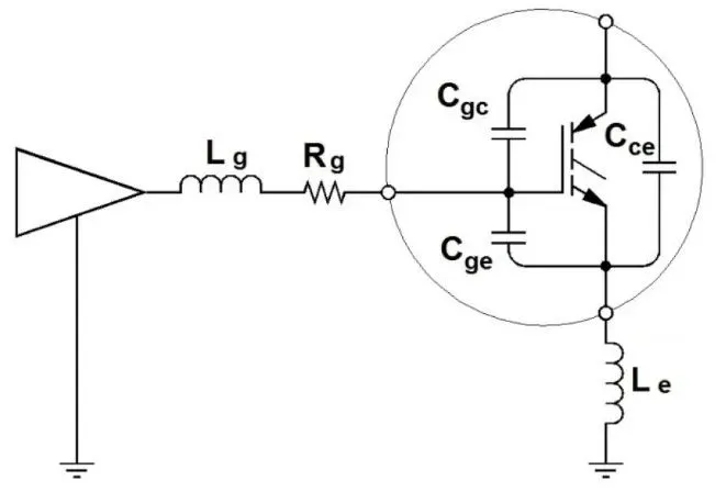
Characteristic Curves
Characteristic curves describe the relationships between electrode voltages and currents for a transistor and are used to analyze its operating behavior. Common curves include input characteristics and output characteristics. The following analysis uses a common-emitter circuit as the reference.
Input characteristic: This curve shows the relationship between the input current (base current Ib) and the input voltage (base-emitter voltage Ube) when the emitter-collector voltage Uec is held constant.
Output characteristic: The output characteristic shows the relationship between output voltage uCE and output current iC for a fixed base current IB.
Key Parameters
Important transistor parameters to consider when selecting a device include current gain (also called current amplification factor), power dissipation, reverse current, and other electrical limits.
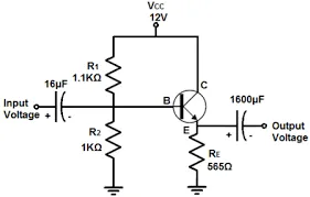
Applications
The most common application for transistors is switching circuits, where they operate as electronic switches or amplifiers in analog and digital systems.