ALLPCB


If you're dealing with BGA rework defects like solder bridging, voiding, misalignment, or open circuits, you're in the right place. This guide offers practical solutions to identify and fix these issues, ensuring reliable results in your PCB assembly process. Whether you're a seasoned engineer or new to Ball Grid Array (BGA) rework, we'll walk you through the most common problems and provide actionable tips to overcome them. Let's dive into the details of troubleshooting BGA rework defects and achieving high-quality soldering outcomes.
What Are BGA Rework Defects and Why Do They Matter?
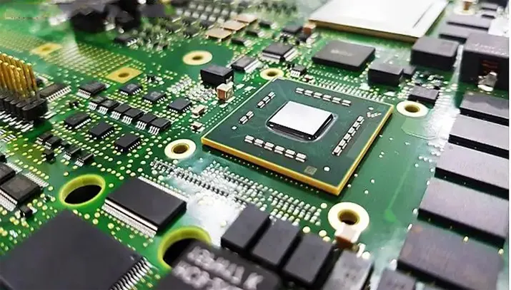
BGA components are widely used in modern electronics due to their high pin density and compact design. However, reworking these components—whether for repair or replacement—can be challenging. Defects during BGA rework can lead to poor connections, reduced reliability, and even complete device failure. Common issues include solder bridging, voiding, misalignment, and open circuits, each of which can compromise the performance of your PCB.
Understanding and troubleshooting these defects is crucial for maintaining product quality and avoiding costly rework cycles. In this guide, we'll break down each defect, explore its causes, and provide practical solutions to help you achieve flawless BGA rework. By addressing these issues head-on, you can improve yield rates and ensure long-term reliability for your electronic assemblies.
Understanding BGA Rework: The Basics
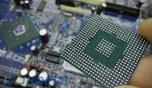
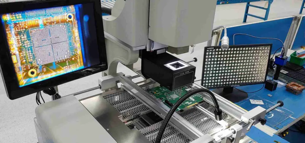
Before diving into specific defects, let's cover the basics of BGA rework. BGA components are soldered to a PCB using an array of tiny solder balls beneath the package. During rework, the component is removed, the site is cleaned, and a new component is soldered in place. This process requires precision, as even small errors in temperature control, alignment, or solder application can lead to defects.
Rework typically involves specialized equipment like hot air stations or infrared heaters to melt the solder, along with tools for precise placement and inspection. However, despite best efforts, defects can still occur due to factors like improper heating profiles, inadequate flux application, or mechanical misalignment. Let's explore the most common BGA rework defects and how to troubleshoot them effectively.
Common BGA Rework Defects and Their Solutions
1. BGA Rework Solder Bridging: Causes and Fixes
Solder bridging occurs when excess solder creates unintended connections between adjacent solder balls, leading to short circuits. This defect is often caused by excessive solder paste, improper stencil design, or uneven heating during reflow.
Causes of Solder Bridging:
- Too much solder paste applied during rework, often due to oversized stencil apertures.
- Uneven heating, causing solder to flow unpredictably and connect neighboring balls.
- Inadequate flux, which fails to prevent solder from spreading beyond its intended area.
Troubleshooting Tips for Solder Bridging:
- Refine Stencil Design: Ensure stencil apertures are sized correctly, typically 10-20% smaller than the pad diameter, to control solder volume.
- Optimize Reflow Profile: Use a gradual ramp-up in temperature (e.g., 2-3°C per second) to prevent sudden solder flow. Maintain a peak temperature around 220-245°C for lead-free solder, depending on the alloy.
- Use Adequate Flux: Apply a thin, even layer of flux to reduce surface tension and prevent solder from spreading.
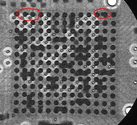
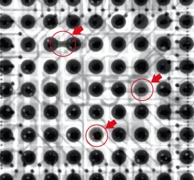
- Inspect Post-Rework: Use X-ray inspection to detect hidden bridges beneath the BGA package. If bridging is found, carefully remove excess solder with a fine-tip soldering iron and wick.
2. BGA Rework Voiding: Identifying and Reducing Air Pockets
Voiding refers to the formation of air or gas pockets within the solder joint, which can weaken the connection and reduce thermal and electrical conductivity. Voids often form during the reflow process when trapped gases fail to escape before the solder solidifies.
Causes of Voiding:
- Insufficient soak time during reflow, preventing gases from escaping.
- Moisture in the PCB or component, which vaporizes and creates voids.
- Poor solder paste quality or excessive flux outgassing.
Troubleshooting Tips for Voiding:
- Extend Soak Phase: Adjust your reflow profile to include a soak phase of 90-120 seconds at 150-180°C. This allows gases to escape before the solder reaches liquidus temperature.
- Bake Components: Pre-bake the PCB and BGA component at 125°C for 4-6 hours to remove moisture before rework.
- Use High-Quality Solder Paste: Choose a paste with low outgassing properties and store it properly to avoid degradation.
- Inspect with X-ray: Voids are not visible to the naked eye. Use X-ray imaging to assess void percentage—aim for less than 25% voiding per joint as per industry standards like IPC-A-610.
3. BGA Rework Misalignment: Preventing Placement Errors
Misalignment happens when the BGA component is not placed accurately on the PCB pads, resulting in open circuits or weak joints. This defect can occur during manual placement or due to equipment calibration issues.
Causes of Misalignment:
- Inaccurate placement equipment or lack of fiducial marks for alignment reference.
- Human error during manual rework processes.
- Warped PCB or component, preventing proper contact during placement.
Troubleshooting Tips for Misalignment:
- Calibrate Equipment: Regularly calibrate placement machines to ensure accuracy within 0.01mm for high-precision BGA components.
- Use Fiducial Marks: Ensure clear and visible fiducial marks on the PCB for automated alignment. These reference points help machines position the BGA correctly.
- Post-Placement Inspection: Use a high-resolution camera or optical inspection system to verify alignment before reflow. Correct any offset immediately.
- Check for Warpage: Inspect the PCB and component for warpage using a flatness gauge. If warpage exceeds 0.1mm, consider replacing the affected part or using a specialized fixture during rework.
4. BGA Rework Open Circuits: Diagnosing and Repairing Failed Connections
Open circuits occur when one or more solder balls fail to connect with the PCB pad, often due to insufficient solder, poor wetting, or mechanical stress. This defect results in incomplete electrical connections, causing device malfunction.
Causes of Open Circuits:
- Insufficient solder paste volume, leaving some balls without enough material to form a joint.
- Poor wetting due to oxidized pads or inadequate flux application.
- Mechanical stress during cooling, causing solder joints to crack or separate.
Troubleshooting Tips for Open Circuits:
- Verify Solder Volume: Check stencil thickness and aperture size to ensure adequate solder paste deposition, typically 0.1-0.15mm thick for standard BGA pads.
- Clean and Flux Pads: Remove oxidation from PCB pads using a mild abrasive or chemical cleaner, then apply flux to improve wetting during reflow.
- Control Cooling Rate: Avoid rapid cooling after reflow, as it can induce thermal stress. Aim for a cooling rate of 2-4°C per second to minimize joint cracking.
- Inspect with X-ray or Testing: Use X-ray imaging to identify open circuits beneath the BGA. Alternatively, perform electrical testing to confirm connectivity across all pins.
General Best Practices for Preventing BGA Rework Defects
While troubleshooting specific defects is essential, adopting best practices can prevent issues from arising in the first place. Here are some universal tips to enhance your BGA rework process:
- Use Proper Equipment: Invest in high-quality rework stations with precise temperature control and placement accuracy. Ensure your tools are calibrated regularly.
- Follow Reflow Profiles Guidelines: Adhere to manufacturer-recommended reflow profiles for the specific solder alloy and component. Avoid deviations that could cause thermal shock or uneven heating.
- Maintain a Clean Work Environment: Contaminants like dust or residue can interfere with solder joints. Keep your workspace clean and handle components with care.
- Train Personnel: Ensure all team members are trained in BGA rework techniques and understand the importance of precision and process control.
- Document and Analyze: Keep detailed records of rework processes and outcomes. Analyze defect trends to identify recurring issues and implement corrective measures.
Advanced Inspection Techniques for BGA Rework Defects
Since BGA solder joints are hidden beneath the component, visual inspection alone isn't enough. Advanced techniques like X-ray inspection are critical for detecting defects such as bridging, voiding, and open circuits. Here's how to leverage inspection tools effectively:
- X-ray Inspection: Use automated X-ray systems to examine solder ball connections. Look for irregularities in shape, size, or spacing. Most systems can quantify void percentages, helping you meet standards like IPC-7095, which recommends less than 25% voiding for critical applications.
- Electrical Testing: Perform in-circuit testing to verify connectivity and identify open circuits or shorts. Use test fixtures designed for BGA packages to ensure accurate results.
- Thermal Imaging: Use thermal cameras to detect uneven heating or hot spots during reflow, which can indicate potential defects like voiding or poor wetting.
By integrating these inspection methods into your workflow, you can catch defects early and reduce the need for extensive rework.
Conclusion: Mastering BGA Rework for Reliable Results
Troubleshooting BGA rework defects like solder bridging, voiding, misalignment, and open circuits requires a combination of precision, proper equipment, and process control. By understanding the root causes of these issues and applying the practical solutions outlined in this guide, you can significantly improve the quality of your BGA rework outcomes. From optimizing reflow profiles to using advanced inspection techniques, every step plays a crucial role in ensuring reliable solder joints and long-lasting electronic assemblies.
Implementing best practices and staying vigilant during the rework process will help you minimize defects and boost efficiency. With the tips and strategies provided here, you're well-equipped to tackle even the most challenging BGA rework defects and achieve consistent, high-quality results in your PCB projects.