In the world of PCB design and manufacturing, pad-to-pad spacing is a critical factor that can make or break the quality of soldering and the ease of rework. Whether you're dealing with PCB soldering defects, facing rework challenges with pad spacing, or aiming to prevent issues like the tombstoning effect, understanding and optimizing pad spacing is essential. This guide dives deep into the best practices for pad-to-pad spacing, covering key aspects like thermal relief pad design and wave soldering spacing requirements. Let’s explore how to design for success and minimize costly errors in your PCB projects.
What Is Pad-to-Pad Spacing and Why Does It Matter?
Pad-to-pad spacing refers to the distance between the centers of two adjacent solder pads on a printed circuit board (PCB). This seemingly small detail plays a huge role in determining the quality of soldering, the density of component placement, and the overall reliability of the board. Proper spacing ensures that components are soldered correctly without defects, while inadequate spacing can lead to issues like solder bridging, poor connections, or challenges during rework.
Optimizing pad-to-pad spacing is not just about fitting more components onto a board. It’s about striking a balance between design density, manufacturability, and performance. In this blog, we’ll break down the importance of spacing, common problems associated with poor design, and actionable tips to get it right for both manual and automated soldering processes.
The Impact of Pad-to-Pad Spacing on Soldering Quality
Soldering is the backbone of PCB assembly, and pad spacing directly affects how well solder adheres to pads and components. Let’s look at how spacing influences common soldering outcomes and defects.
Preventing Solder Bridging
Solder bridging occurs when excess solder creates an unintended connection between two pads, leading to short circuits. This is a common issue in designs with tight pad spacing, especially in surface-mount technology (SMT) assemblies. For instance, if the spacing between pads is less than 0.2 mm for fine-pitch components, the risk of bridging increases significantly due to the small margin for error during solder paste application.
To avoid this, ensure that pad spacing adheres to the minimum requirements based on your soldering process. For SMT components, a general rule of thumb is to maintain a center-to-center spacing of at least 0.25 mm for 0402 packages and above, adjusting for smaller or larger components as needed.
Reducing the Tombstoning Effect
The tombstoning effect is a defect where one end of a surface-mount component lifts off the pad during reflow soldering, resembling a tombstone. This often happens due to uneven heating or improper pad spacing. If pads are too close together or unevenly sized, the solder may melt at different rates, pulling the component out of alignment.
To mitigate tombstoning, maintain consistent pad sizes and ensure a minimum spacing that allows for even heat distribution. For small chip components like resistors and capacitors, a spacing of 0.3 mm or more between pads can help, depending on the component size and soldering method.
Rework Challenges with Pad Spacing: What You Need to Know
Reworking a PCB—removing and replacing components—can be a nightmare if pad spacing isn’t optimized. Tight spacing makes it difficult to access individual pads with soldering tools, increasing the risk of damaging nearby components or traces. Let’s explore the rework challenges with pad spacing and how to address them.
Accessibility Issues During Rework
When pads are placed too closely together, using a soldering iron or hot air rework station becomes tricky. For example, with a spacing of less than 0.5 mm, there’s a high chance of accidentally desoldering adjacent components or overheating the board. This is especially problematic in high-density designs where components are packed tightly.
To ease rework, aim for a pad-to-pad spacing that allows at least 0.8 mm of clearance for manual soldering tools. If your design must use tighter spacing, consider using automated rework equipment with precision tips to minimize damage.
Thermal Stress and Pad Damage
Rework often involves applying heat to remove or resolder components, which can stress the PCB if pads are too close to each other. Heat can spread to adjacent pads, weakening solder joints or lifting pads off the board. Incorporating thermal relief pad design can help by reducing heat transfer to surrounding areas, making rework safer and more effective.
Thermal Relief Pad Design: A Key to Better Soldering and Rework
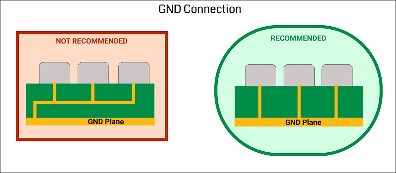
Thermal relief pads are a design technique used to manage heat distribution during soldering and rework. They feature small copper spokes connecting the pad to a larger copper plane, limiting heat dissipation to prevent thermal stress. This is particularly useful for through-hole components or pads connected to large ground planes.
Benefits of Thermal Relief Pads
Thermal relief pads ensure that heat stays localized during soldering, allowing for consistent solder flow without overheating nearby areas. For instance, without thermal relief, a pad connected to a ground plane might require excessive heat to melt solder, risking damage to the component or board. With thermal relief, the heat focuses on the pad, often reducing soldering time by 20-30% in some cases.
Design Tips for Thermal Relief
When designing thermal relief pads, use 2-4 spokes per pad with a width of about 0.2-0.3 mm to balance thermal isolation and electrical connectivity. Ensure the spacing between the pad and the copper plane allows for effective heat management without compromising the connection. This approach is critical for both reflow and wave soldering spacing requirements.
Wave Soldering Spacing Requirements: Getting It Right
Wave soldering, commonly used for through-hole components, has specific wave soldering spacing requirements to ensure quality and prevent defects. Unlike reflow soldering, wave soldering involves passing the PCB over a molten solder wave, which can create unique challenges if pad spacing isn’t optimized.
Minimum Spacing for Wave Soldering
For wave soldering, pad-to-pad spacing should generally be at least 1.5-2.0 mm to prevent solder bridging as the wave passes over the board. Closer spacing can cause excess solder to accumulate between pads, leading to shorts. Additionally, ensure that pads are oriented perpendicular to the direction of the solder wave to minimize shadowing effects, where components block solder from reaching certain pads.
Component Orientation and Spacing
Proper component orientation is just as important as spacing in wave soldering. Place larger components downstream of smaller ones in the solder wave direction to avoid interference. Maintain a spacing of at least 2.5 mm between through-hole pads and adjacent SMT pads to prevent solder wicking or uneven flow.
Common PCB Soldering Defects Linked to Pad Spacing
Poor pad spacing is often the root cause of many PCB soldering defects. Understanding these issues can help you design better layouts and reduce manufacturing errors. Below are some frequent defects tied to spacing problems.
Insufficient Solder Joints
If pads are spaced too far apart for a component, the solder may not form a strong joint, leading to weak connections or open circuits. For SMT components, ensure pad spacing matches the component footprint specifications, typically within a tolerance of 0.1 mm, to guarantee proper solder coverage.
Excess Solder and Bridging
As mentioned earlier, tight spacing increases the risk of excess solder forming bridges between pads. This is particularly common in fine-pitch designs where spacing is below 0.2 mm. Using a well-designed solder mask and maintaining adequate spacing can prevent this issue during assembly.
Best Practices for Optimizing Pad-to-Pad Spacing
Now that we’ve covered the challenges and defects related to pad spacing, let’s dive into actionable best practices to optimize your PCB design for soldering and rework.
Follow Industry Standards
Adhere to guidelines from standards like IPC-7351 for pad spacing and footprint design. These standards provide recommended spacing for various component types and soldering processes, ensuring compatibility with most manufacturing setups. For example, IPC suggests a minimum pad-to-pad spacing of 0.25 mm for SMT components to avoid bridging.
Use Design Software Tools
Leverage PCB design software with built-in design rule checks (DRC) to automatically flag spacing violations. Set custom rules for minimum pad spacing based on your soldering process, whether it’s reflow, wave, or manual soldering, to catch issues before production.
Test and Iterate
Before full-scale production, create prototype boards with varying pad spacings to test soldering quality and rework ease. For instance, test spacings of 0.3 mm, 0.5 mm, and 0.8 mm for SMT components to see which yields the best results under your specific assembly conditions.
How Pad Spacing Affects Signal Integrity
Beyond soldering and rework, pad-to-pad spacing also impacts signal integrity, especially in high-speed designs. Tight spacing can lead to crosstalk or electromagnetic interference (EMI) between adjacent traces or pads, degrading performance.
For high-speed signals, maintain a spacing of at least 3 times the trace width between adjacent pads to minimize crosstalk. For example, if your trace width is 0.1 mm, aim for a pad spacing of 0.3 mm or more. Additionally, consider using ground planes or shielding to further isolate signals in dense layouts.
Conclusion: Master Pad-to-Pad Spacing for Flawless PCBs
Pad-to-pad spacing is a fundamental aspect of PCB design that directly influences soldering quality, rework feasibility, and overall board reliability. By addressing challenges like PCB soldering defects, optimizing for rework challenges with pad spacing, incorporating thermal relief pad design, preventing the tombstoning effect, and meeting wave soldering spacing requirements, you can significantly improve your PCB projects.
Start by following industry standards, testing different spacings, and using design tools to catch errors early. With careful planning and attention to detail, you’ll create boards that are easier to assemble, rework, and maintain—saving time, reducing costs, and ensuring top-notch performance. Keep these tips in mind for your next design, and watch your manufacturing process become smoother and more efficient.
 ALLPCB


