ALLPCB


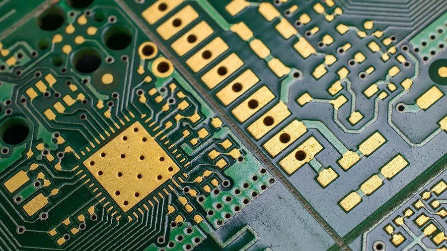
In the world of Surface Mount Technology (SMT) PCB design, solder mask plays a critical role in ensuring the reliability and performance of printed circuit boards. But what exactly is a solder mask, and why is it so important? Simply put, a solder mask is a protective layer applied to a PCB to shield copper traces from oxidation, prevent unintended solder connections, and improve the board's durability. In SMT PCB design, where components are densely packed and precision is key, the solder mask is essential for preventing issues like solder bridging and ensuring accurate assembly.
In this comprehensive guide, we'll dive deep into the significance of solder mask in SMT PCB design. We'll explore topics like solder mask defined pads, non-solder mask defined pads, solder mask materials, solder mask application techniques, and how it helps in preventing solder bridging. Whether you're a seasoned engineer or new to PCB design, this post will provide valuable insights to help you optimize your designs for better performance and manufacturability.
What Is a Solder Mask and Why Does It Matter in SMT PCB Design?
A solder mask, often referred to as solder resist, is a thin polymer layer applied to the surface of a PCB. Its primary purpose is to protect the copper traces from environmental factors like moisture and dust, which can cause oxidation and degrade the board over time. In SMT PCB design, where components are soldered directly onto the board's surface, the solder mask also prevents solder from flowing to unintended areas during assembly.
In SMT designs, components are smaller and placed closer together compared to traditional through-hole technology. This high density increases the risk of short circuits if solder accidentally connects adjacent pads or traces. A properly applied solder mask acts as a barrier, ensuring that solder only adheres to designated areas, such as component pads. Without it, the risk of defects during manufacturing skyrockets, leading to costly rework or complete board failure.
Solder Mask Defined Pads vs. Non-Solder Mask Defined Pads
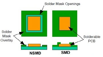
One of the key decisions in SMT PCB design is whether to use solder mask defined pads (SMD) or non-solder mask defined pads (NSMD). Both approaches impact how solder interacts with the pads during assembly, affecting the reliability of the solder joints.
What Are Solder Mask Defined Pads?
Solder mask defined pads (SMD) are pads where the solder mask overlaps the edges of the copper pad, reducing the exposed copper area. This overlap creates a smaller opening for solder to adhere to, which can help control the amount of solder applied during the reflow process. SMD pads are often used in designs where precision is critical, as they minimize the risk of solder bridging between closely spaced pads. For instance, in fine-pitch components with pad spacing as small as 0.5mm, SMD pads can prevent excess solder from spreading to adjacent areas.
What Are Non-Solder Mask Defined Pads?
Non-solder mask defined pads (NSMD), on the other hand, have the solder mask pulled back from the copper pad, exposing the entire pad and sometimes a small area around it. This design allows for a larger solderable area, which can improve the strength of the solder joint. NSMD pads are commonly used for components like ball grid arrays (BGAs), where strong mechanical connections are needed to withstand thermal and mechanical stress. Studies suggest that NSMD pads can increase solder joint reliability by up to 20% in high-stress applications compared to SMD pads.
Choosing Between SMD and NSMD Pads
The choice between SMD and NSMD pads depends on the specific requirements of your SMT design. If your design prioritizes preventing solder bridging in densely packed areas, SMD pads may be the better option. However, for components that require robust solder joints, such as those in high-vibration environments, NSMD pads offer better performance. Understanding the trade-offs between these two approaches is crucial for optimizing your PCB layout.
Solder Mask Materials: What You Need to Know
The effectiveness of a solder mask in SMT PCB design largely depends on the material used. Different solder mask materials offer varying levels of protection, thermal resistance, and ease of application. Here are the most common types used in the industry:
- Liquid Photoimageable (LPI) Solder Mask: This is the most widely used solder mask material due to its precision and versatility. LPI solder mask is applied as a liquid and cured using UV light, allowing for high-resolution patterns. It can withstand temperatures up to 260°C during reflow soldering, making it ideal for SMT processes.
- Dry Film Solder Mask: This material comes in a solid film form and is laminated onto the PCB. While it offers excellent thickness uniformity, it is less common in SMT designs due to its lower resolution compared to LPI. It's often used in simpler designs with larger feature sizes.
- Epoxy-Based Solder Mask: Known for its durability, epoxy-based solder mask is resistant to harsh chemicals and mechanical wear. However, it may not offer the same precision as LPI for fine-pitch SMT components.
Choosing the right solder mask material is vital for ensuring the longevity and performance of your PCB. For high-density SMT designs, LPI solder mask is often the preferred choice due to its ability to create precise openings for pads as small as 0.1mm in diameter.
Solder Mask Application Techniques in SMT PCB Design
The process of applying solder mask to a PCB is just as important as the material itself. Proper solder mask application ensures that the protective layer adheres well to the board and covers all necessary areas without defects. Here’s a step-by-step overview of the typical application process for SMT PCBs:
- Surface Preparation: The PCB surface is cleaned to remove contaminants like dust or oil that could prevent the solder mask from adhering properly. This step is critical to avoid defects like peeling or uneven coating.
- Coating Application: Depending on the material, the solder mask is applied as a liquid (for LPI) or laminated as a film (for dry film). For LPI, the liquid is sprayed or rolled onto the board to achieve a uniform thickness, typically between 0.02mm and 0.04mm.
- Exposure and Development: For photoimageable solder masks, the coated PCB is exposed to UV light through a photomask, which defines the areas where the solder mask will remain. Unexposed areas are then washed away during development, leaving openings for pads and vias.
- Curing: The solder mask is cured using heat or UV light to harden the material and ensure it bonds securely to the PCB. This step enhances the mask's resistance to high temperatures during SMT soldering, often exceeding 250°C.
Precision in solder mask application is especially important in SMT designs, where even a slight misalignment can cover part of a pad, leading to poor solder joints. Advanced manufacturing processes use automated equipment to achieve alignment accuracy within 0.05mm, ensuring reliable results for fine-pitch components.

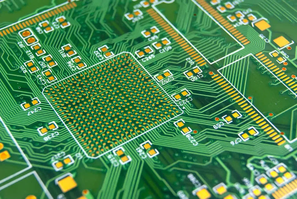
Preventing Solder Bridging with Solder Mask
Solder bridging is a common defect in SMT PCB assembly, where excess solder creates an unintended connection between two adjacent pads or traces, causing a short circuit. This issue is particularly problematic in designs with fine-pitch components, where pad spacing can be as tight as 0.4mm. The solder mask plays a pivotal role in preventing solder bridging by acting as a physical barrier that confines solder to the intended areas.
Here’s how solder mask helps in preventing solder bridging:
- Isolating Pads: By covering the areas between pads, the solder mask prevents solder from flowing outside the designated soldering zones during reflow. This is crucial for components like quad flat packages (QFPs) with lead spacing below 0.5mm.
- Controlling Solder Volume: In solder mask defined pads, the mask opening limits the amount of solder that can be applied, reducing the risk of excess solder spilling over to nearby pads.
- Improving Assembly Accuracy: A well-designed solder mask ensures that solder paste stencils align precisely with the pads, minimizing the chance of misplaced solder that could lead to bridging.
In addition to using solder mask, designers can further reduce solder bridging risks by optimizing pad spacing and stencil design. For instance, increasing the spacing between pads to at least 0.2mm beyond the minimum requirement can provide an extra margin of safety in high-density SMT layouts.
Best Practices for Solder Mask Design in SMT PCBs
To maximize the benefits of solder mask in SMT PCB design, engineers should follow these best practices:
- Ensure Adequate Clearance: Maintain a clearance of at least 0.1mm between the solder mask edge and the copper pad for NSMD designs to avoid mask encroachment on the solderable area.
- Use High-Resolution Materials: Opt for LPI solder mask for fine-pitch designs to achieve precise openings and avoid defects in densely packed areas.
- Verify Alignment: Double-check the alignment of the solder mask layer with the copper layer during design reviews to prevent misregistration, which can expose traces or cover pads.
- Consider Thermal Expansion: Account for the thermal expansion of the solder mask material during reflow soldering, as mismatched expansion rates can lead to cracks or delamination.
Following these guidelines can significantly improve the reliability of your SMT PCB design, reducing the likelihood of manufacturing defects and ensuring consistent performance in the final product.
Conclusion: Why Solder Mask Is a Game-Changer in SMT PCB Design
In SMT PCB design, the solder mask is far more than just a protective coating—it’s a critical element that impacts the manufacturability, reliability, and performance of the board. From defining solder mask defined pads and non-solder mask defined pads to selecting the right solder mask materials and mastering application techniques, every aspect of solder mask design influences the success of your project. Most importantly, its role in preventing solder bridging ensures that your high-density designs remain free from short circuits and other assembly defects.
By understanding the nuances of solder mask and incorporating best practices into your design process, you can create SMT PCBs that meet the highest standards of quality and durability. Whether you're working on consumer electronics, automotive systems, or industrial equipment, a well-implemented solder mask is the foundation of a robust and reliable PCB.
At ALLPCB, we’re committed to helping you achieve excellence in PCB design and manufacturing. With our expertise and advanced processes, you can trust that your SMT designs will benefit from precision solder mask application and top-notch quality control. Let’s work together to bring your innovative ideas to life with PCBs that perform flawlessly in any application.