 ALLPCB


Electrostatic discharge (ESD) is a silent danger in the world of PCB assembly, often causing damage that isn’t immediately visible. Latent ESD defects in PCBs can lead to long-term reliability issues, unexpected failures, and costly repairs. In this blog, we dive deep into what latent ESD damage is, how it affects surface mount technology (SMT) processes, and how to detect and prevent it. Whether you’re an engineer or a manufacturer, understanding ESD-induced reliability issues and implementing effective control methods is crucial for ensuring the longevity of your electronic products.
What Is Latent ESD Damage in PCB Assembly?
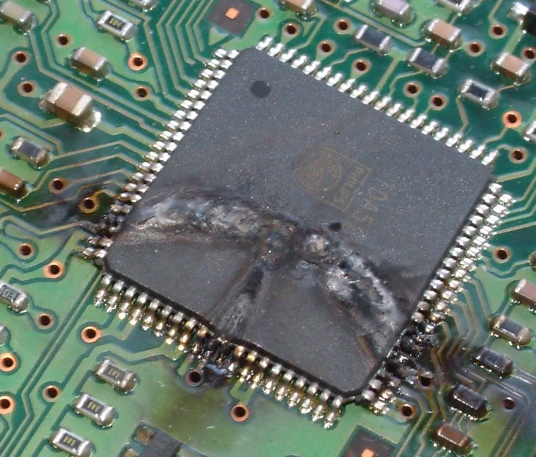
Latent ESD damage refers to hidden harm caused by electrostatic discharge that doesn’t immediately result in a failure. Unlike catastrophic ESD damage, which causes instant component breakdown, latent damage weakens components over time, leading to premature failure. This type of damage often goes undetected during initial testing, making it a significant threat to long-term reliability in PCB assembly.
In PCB manufacturing, particularly during SMT processes, sensitive components like integrated circuits (ICs), capacitors, and transistors are at risk. A small ESD event—sometimes as low as 100 volts—can create micro-cracks in a component’s oxide layer or degrade its internal junctions. Over time, these defects worsen under operational stress, leading to intermittent failures or complete breakdowns months or even years later.
Why Latent ESD Defects Matter in PCB Assembly
Latent ESD defects in PCBs are a critical concern because they compromise the reliability of electronic devices. For industries like automotive, aerospace, and medical, where safety and performance are non-negotiable, a single failure can have severe consequences. According to industry studies, up to 90% of ESD-related failures are due to latent damage rather than immediate catastrophic events.
These defects can cause:
- Intermittent Failures: Devices may work initially but fail sporadically during use.
- Reduced Lifespan: Components degrade faster, shortening the product’s overall life.
- Costly Recalls: Failures in the field often lead to expensive repairs or replacements.
Understanding and addressing latent ESD damage is essential for maintaining trust with customers and ensuring compliance with strict industry standards.
How Latent ESD Damage Occurs During SMT Assembly
Surface mount technology (SMT) assembly involves handling tiny, highly sensitive components that are prone to ESD damage. Latent defects often occur due to improper handling, inadequate grounding, or insufficient protective measures during manufacturing. Here are some common causes:
- Human Handling: A worker’s body can carry a static charge of up to 3,000 volts, far exceeding the 100-volt threshold that can harm sensitive components.
- Equipment Issues: Ungrounded soldering irons or automated pick-and-place machines can transfer static charges to components.
- Environmental Factors: Low humidity environments increase static buildup, raising the risk of ESD events.
- Packaging and Storage: Improperly shielded packaging can allow static charges to accumulate and discharge during handling.
During SMT assembly, even a minor ESD event can create latent damage by stressing a component’s internal structure. For example, a capacitor might suffer a tiny breach in its dielectric layer, reducing its ability to store charge over time. These issues often remain hidden until the component is subjected to thermal or electrical stress during operation.
Detecting ESD Damage in SMT: Challenges and Methods
Detecting ESD damage in SMT components is challenging because latent defects are not immediately apparent. Standard electrical tests, such as in-circuit testing (ICT), may not reveal issues since the component might still function within acceptable parameters initially. However, there are advanced methods to identify potential problems:
- Microscopic Inspection: High-powered microscopes can reveal physical signs of damage, such as micro-cracks or melted junctions, on a component’s surface.
- Thermal Imaging: Infrared cameras can detect abnormal heat patterns in components, indicating internal stress or degradation caused by ESD.
- Transmission Line Pulsing (TLP): This technique applies controlled pulses to components to simulate ESD events and measure their response, helping identify latent weaknesses.
- Leakage Current Testing: Measuring small changes in leakage current can indicate damage to insulating layers within components.
While these methods are effective, they require specialized equipment and expertise, making them costly for small-scale manufacturers. Prevention, therefore, remains the most practical approach for addressing latent ESD defects in PCBs.
ESD-Induced Reliability Issues: Long-Term Impact on PCBs
ESD-induced reliability issues can manifest in various ways, depending on the component and the severity of the latent damage. Some common long-term effects include:
- Signal Integrity Problems: Damaged components may cause noise or distortion in high-speed circuits, affecting data transmission. For instance, a damaged IC in a 5G communication device might struggle to maintain signal integrity at frequencies above 3 GHz.
- Power Failures: Latent damage in power management components can lead to inefficient power distribution, causing overheating or shutdowns.
- Thermal Stress: Micro-cracks caused by ESD can expand under thermal cycling, leading to complete failure. A component rated for 85°C operation might fail at 70°C due to underlying damage.
These issues often surface after a product has been deployed, making it difficult to trace the root cause back to an ESD event during assembly. This delayed failure pattern underscores the importance of robust ESD control measures during manufacturing.
PCB Failure Analysis for ESD: Identifying the Root Cause
PCB failure analysis for ESD involves a systematic approach to pinpoint whether latent damage is the cause of a malfunction. Engineers typically follow these steps:
- Visual Inspection: Check for physical signs of damage, such as discoloration or cracks, on components and traces.
- Electrical Testing: Measure parameters like resistance, capacitance, and leakage current to identify deviations from expected values.
- Environmental Testing: Subject the PCB to thermal and humidity stress to accelerate latent defects and observe failure patterns.
- Advanced Imaging: Use X-ray or scanning electron microscopy (SEM) to examine internal structures for hidden damage.
Failure analysis not only helps identify ESD as the culprit but also provides insights into process weaknesses. For instance, if multiple failures occur in components handled by a specific machine, it may indicate improper grounding or static buildup in that equipment.
Long-Term Reliability Through ESD Control: Best Practices
Ensuring long-term reliability with ESD control requires a proactive approach during every stage of PCB assembly. Here are actionable best practices to minimize the risk of latent ESD damage:
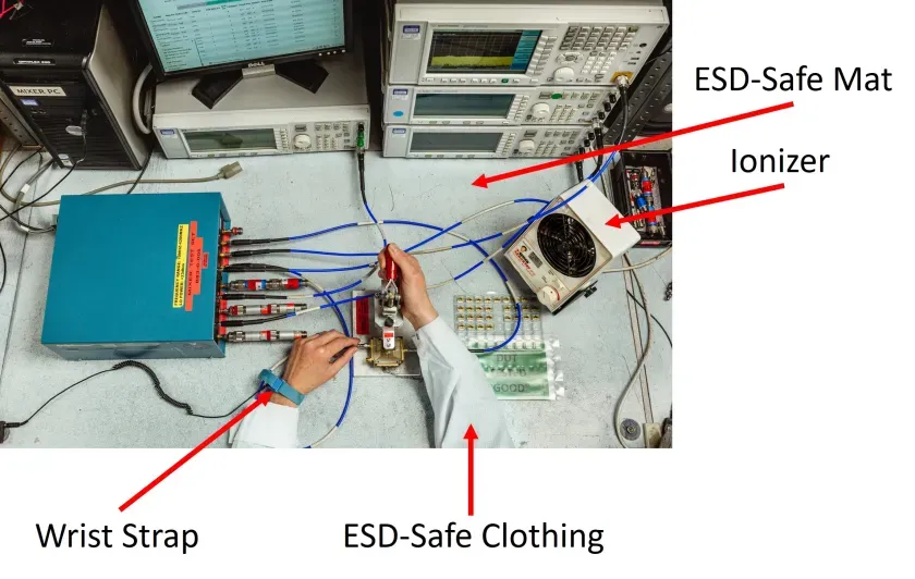
- Workstation Grounding: Equip all workstations with grounded mats and wrist straps to dissipate static charges. Ensure resistance to ground is below 10^9 ohms for effective protection.
- ESD-Safe Tools: Use ESD-safe soldering irons, tweezers, and other tools to prevent static discharge during handling.
- Environmental Control: Maintain humidity levels between 40-60% in assembly areas to reduce static buildup.
- Protective Packaging: Store and transport components in ESD-shielded bags or containers to prevent charge accumulation.
- Training Programs: Educate staff on proper ESD handling procedures to minimize human-induced risks.
- Regular Audits: Conduct periodic checks on ESD control measures to ensure compliance with standards like ANSI/ESD S20.20.
Implementing these measures can significantly reduce the occurrence of latent ESD defects, enhancing the reliability of your PCBs over time.
The Cost of Ignoring Latent ESD Damage
Neglecting latent ESD damage can have severe financial and reputational consequences. A single batch of defective PCBs can lead to millions of dollars in recalls, especially for high-stakes applications like medical devices or automotive systems. Beyond direct costs, repeated failures erode customer trust, making it harder to maintain a competitive edge in the market.
Investing in ESD prevention is far more cost-effective than dealing with the aftermath of failures. For example, the cost of setting up an ESD-safe workstation—typically under $500—pales in comparison to the potential loss from a single product recall.
Conclusion: Safeguarding Your PCBs Against Latent ESD Damage
Latent ESD damage in PCB assembly is a hidden threat that can undermine the reliability and performance of electronic products. By understanding how these defects occur, implementing robust detection methods, and prioritizing ESD control, manufacturers can protect their components from long-term reliability issues. From grounding workstations to using protective packaging, every step counts in minimizing the risk of ESD-induced failures.
At ALLPCB, we are committed to helping you achieve the highest standards of quality and reliability in your PCB projects. By staying vigilant and adopting best practices, you can ensure your products stand the test of time, delivering consistent performance to your customers.


