 ALLPCB


In the world of high-speed digital PCBs, impedance matching is a critical skill for ensuring signal integrity and minimizing reflections. If you're designing circuits for fast data rates, like those in modern communication systems or computing devices, understanding high-speed PCB impedance can make or break your design. Poor impedance control leads to signal reflections, data loss, and degraded performance. This blog post dives deep into the essentials of impedance matching, exploring concepts like the signal reflection coefficient, controlled impedance routing, differential impedance calculation, and TDR impedance measurement. Let's explore how to master these techniques for optimal PCB performance.
What Is Impedance Matching and Why Does It Matter?
Impedance matching is the process of designing a PCB so that the impedance of the transmission lines matches the source and load impedances. When these values align, signals travel smoothly without bouncing back as reflections. Reflections occur when there's a mismatch, causing part of the signal to return to the source, which can distort data and introduce errors in high-speed systems.
In high-speed digital designs, such as those operating at frequencies above 100 MHz or with data rates exceeding 1 Gbps, even small mismatches can create significant issues. For instance, a mismatched trace on a PCB can cause signal delays, crosstalk, or electromagnetic interference (EMI). By mastering high-speed PCB impedance, designers can ensure reliable performance in applications like USB, HDMI, or DDR memory interfaces.
Understanding the Signal Reflection Coefficient
The signal reflection coefficient is a measure of how much of a signal is reflected back due to an impedance mismatch. It's calculated using the formula:
Reflection Coefficient (Γ) = (Z_load - Z_source) / (Z_load + Z_source)
Here, Z_load is the impedance of the load, and Z_source is the impedance of the source or transmission line. If the reflection coefficient is zero, it means there's no reflection, and the impedances are perfectly matched. A value closer to 1 or -1 indicates a severe mismatch, leading to significant signal loss.
For example, if a transmission line has an impedance of 50 ohms (a common standard in high-speed designs) and the load is 75 ohms, the reflection coefficient would be (75 - 50) / (75 + 50) = 0.2. This means 20% of the signal is reflected, which can degrade performance in high-speed systems. Minimizing this coefficient through proper design is essential for maintaining signal integrity.
The Basics of Controlled Impedance Routing
Controlled impedance routing is a technique used to maintain a consistent impedance along the length of a PCB trace. This is crucial for high-speed signals, where even small variations in trace width, spacing, or dielectric material can alter impedance and cause reflections.
To achieve controlled impedance, designers must consider several factors:
- Trace Width and Thickness: Wider traces have lower impedance, while narrower traces have higher impedance. For a 50-ohm trace on a standard FR-4 material, a trace width of around 6 mils might be required, depending on the stackup.
- Dielectric Constant: The material of the PCB affects impedance. FR-4, with a dielectric constant of about 4.2-4.5, is common, but high-speed designs might use materials like Rogers with lower constants for better performance.
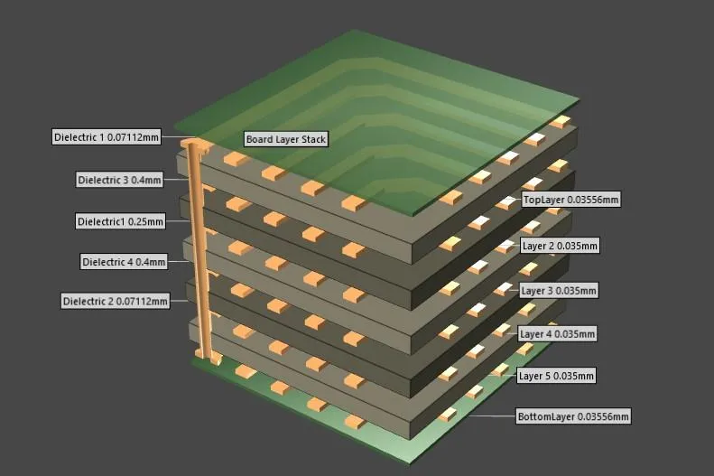
- Layer Stackup: The distance between the trace and the reference plane (ground or power) influences impedance. A thinner dielectric layer increases capacitance, lowering impedance.
Design tools often include impedance calculators to help set these parameters. By adhering to strict design rules during layout, you can ensure that traces maintain the desired impedance, such as 50 ohms for single-ended signals or 100 ohms for differential pairs.
Differential Impedance Calculation for High-Speed Pairs
In many high-speed designs, signals are transmitted as differential pairs, where two traces carry complementary signals. This method reduces noise and improves signal integrity, but it requires precise differential impedance calculation. Differential impedance is the impedance between the two traces of the pair, not to ground, and is typically higher than single-ended impedance.
For example, a common differential impedance for USB or Ethernet interfaces is 90 to 100 ohms. The calculation depends on trace spacing, width, and the dielectric material. The formula for differential impedance is complex, but design software often simplifies it. As a rule of thumb, for a 100-ohm differential pair on FR-4, traces might be 5 mils wide with a spacing of 8 mils, though this varies with stackup.
Key considerations for differential pairs include:
- Equal Lengths: Both traces must be the same length to avoid skew, which can distort the signal.
- Tight Coupling: Traces should be close together to maintain consistent impedance and reduce EMI.
- Avoid Bends: Sharp corners can cause impedance discontinuities, so use smooth curves or 45-degree angles.
By carefully calculating and routing differential pairs, designers can minimize reflections and ensure reliable data transmission at high speeds.
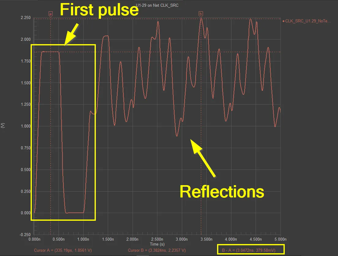
Using TDR for Impedance Measurement
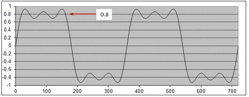
Once a PCB is designed and manufactured, verifying impedance is critical. TDR impedance measurement, or Time Domain Reflectometry, is a powerful technique for this purpose. TDR works by sending a fast electrical pulse down a trace and measuring the reflections that return. The time and amplitude of these reflections indicate impedance discontinuities along the line.
For instance, if a trace is designed for 50 ohms but a section measures 60 ohms due to a manufacturing defect, TDR will show a positive reflection at that point. This allows engineers to identify and correct issues before the board goes into production. Modern TDR equipment can resolve discontinuities with precision down to a few millimeters, making it invaluable for high-speed designs.
TDR is often used in conjunction with other testing methods to ensure the entire board meets specifications. It's especially useful for validating controlled impedance routing and identifying issues in differential pairs.
Practical Tips for Minimizing Signal Reflections
Now that we've covered the core concepts, let's look at actionable strategies to minimize signal reflections in high-speed PCB designs:
- Use Impedance Calculators: Leverage design software to calculate trace dimensions for your target impedance, whether it's 50 ohms for single-ended or 100 ohms for differential signals.
- Choose the Right Materials: Select PCB materials with stable dielectric constants for high-frequency signals. Avoid materials with high loss tangents that can degrade signals.
- Maintain Consistent Routing: Keep trace lengths uniform, especially for differential pairs, to prevent timing skews. Avoid routing over splits in ground planes, as this can alter impedance.
- Terminate Signals Properly: Use termination resistors at the end of transmission lines to match load impedance and absorb reflections. For example, a 50-ohm resistor at the end of a 50-ohm line can prevent bounces.
- Test with TDR: After manufacturing, use TDR to verify impedance across critical traces. Address any discrepancies before final assembly.
Implementing these practices can significantly reduce the signal reflection coefficient and improve overall performance in your high-speed designs.
Common Challenges in High-Speed PCB Impedance Design
Even with the best tools and knowledge, designers face challenges when working with high-speed PCB impedance. Here are a few common issues and how to address them:
- Manufacturing Variations: Small deviations in trace width or dielectric thickness during fabrication can alter impedance. Work closely with your PCB manufacturer to ensure tight tolerances, such as ±10% on trace widths.
- Complex Stackups: Multi-layer boards with varying dielectric heights can complicate impedance control. Use simulation tools to model the stackup and adjust trace dimensions accordingly.
- High-Frequency Effects: At very high frequencies (above 5 GHz), skin effect and dielectric losses become significant. Opt for low-loss materials and wider traces to mitigate these effects.
By anticipating these challenges and planning ahead, you can avoid costly redesigns and ensure your PCB performs as intended.
The Role of Simulation in Impedance Matching
Before sending a design to production, simulation plays a vital role in verifying high-speed PCB impedance. Tools like signal integrity simulators can model how signals will behave on your traces, predicting reflections and crosstalk. For example, a simulation might reveal that a 6-mil trace at 2 GHz has a 3% reflection due to a slight mismatch, allowing you to adjust the design early.
Simulations also help with differential impedance calculation by testing various trace spacings and widths without building physical prototypes. This saves time and reduces errors, ensuring that your design meets performance goals before manufacturing.
Conclusion: Mastering Impedance for High-Speed Success
Impedance matching is an art and a science, essential for any high-speed digital PCB design. By understanding concepts like the signal reflection coefficient, implementing controlled impedance routing, performing accurate differential impedance calculation, and using techniques like TDR impedance measurement, you can minimize signal reflections and achieve reliable performance. Whether you're designing for data rates of 1 Gbps or 10 Gbps, proper impedance control ensures your signals arrive intact, without distortion or loss.
At every stage—from material selection to final testing—attention to detail is key. Use the tips and strategies outlined here to tackle the challenges of high-speed PCB impedance and build boards that meet the demands of modern electronics. With the right approach, you can turn the complex task of impedance matching into a competitive advantage for your designs.


