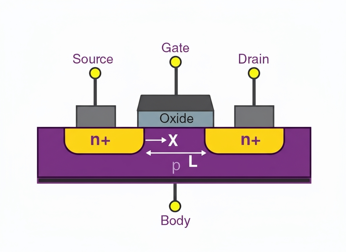
In MOSFET-based circuits, a resistor is often placed in series with the gate. This article examines the purpose of this resistor, specifically why a 100¦¸ resistor is commonly used, and its impact on circuit performance for hardware engineers, PCB designers, and embedded developers.
Purpose of the Gate Resistor
MOSFETs are voltage-controlled devices that require the gate voltage to exceed the threshold voltage to turn on, without needing significant gate current. In theory, no series resistor is required at the gate for MOSFET operation. Additionally, the gate has parasitic capacitance, and to minimize switching losses and achieve faster turn-on and turn-off times, the equivalent gate resistance should ideally be as low as possible, preferably zero.
However, a resistor is frequently included in series with the gate in practical MOSFET circuits. The primary purpose of this resistor is to suppress oscillations during switching transitions. Without it, the MOSFET may experience oscillatory waveforms, which increase switching losses and, in severe cases, could lead to device breakdown due to excessive oscillations.
Why 100¦¸?
The choice of a 100¦¸ resistor is often a practical compromise, determined by the specific MOSFET characteristics and circuit parasitics. Simulation experiments with different gate resistor values illustrate the effects:
- With a 1¦¸ resistor, the drain-source voltage (Vds) exhibits high-frequency oscillations.
- With a 10¦¸ resistor, these oscillations are significantly damped.
- With a 50¦¸ resistor, the rising edge of Vds slows, and the gate voltage shows a plateau due to the Miller capacitance effect between the drain and gate, leading to increased power dissipation in the MOSFET.
A small resistor value may cause output ringing, while a large value extends the switching transition time, increasing power losses. The 100¦¸ value often balances these trade-offs effectively.
Impact of Parasitic Elements and Gate Resistor
In power MOSFET drive circuits, parasitic inductances (e.g., trace or package inductance) interact with the MOSFET¡¯s gate-drain (Cgd) and gate-source (Cgs) capacitances, forming a resonant circuit. This resonance can amplify high-frequency harmonic components in the drive signal, causing fluctuations in the output voltage.
The gate resistor (Rg) increases the damping in the drive circuit, reducing the quality factor (Q) of the resonant circuit formed by the inductance and capacitances. This dampens the resonance, allowing oscillations to decay quickly. The optimal resistor value depends on the specific MOSFET and the circuit¡¯s parasitic inductance.
When Rg is too small, the drive voltage may overshoot significantly, leading to pronounced oscillations, especially with larger parasitic inductances. This can adversely affect the MOSFET and other circuit components. Additionally, a small Rg results in a high peak drive current, which may exceed the current output capability of the driver IC.
Conversely, when Rg is too large, the drive current may reach the maximum output of the driver IC, effectively turning the driver into a constant current source. This leads to linear charging of Cgs, slowing the rise of the drive voltage waveform. A slow-rising drive voltage can negatively impact the MOSFET, particularly when large currents flow through it during switching.
Selecting the Optimal Gate Resistor Value
Choosing an appropriate gate resistor value involves balancing oscillation suppression and switching speed. The value is typically determined based on the MOSFET¡¯s current capacity, voltage rating, and switching frequency, as well as the circuit¡¯s parasitic inductance. A 100¦¸ resistor is often selected as it effectively mitigates oscillations without excessively prolonging the switching transition, minimizing power losses and ensuring reliable operation.
 ALLPCB


