ALLPCB


Introduction
Early IC design focused primarily on performance (timing) and area. EDA tools minimized area while meeting performance requirements, and power was not a major concern.
CMOS processes had very low power consumption at relatively low clock frequencies, with leakage currents negligible. As transistor density and clock frequencies increased, static power from CMOS processes also rose. At the same time, reductions in supply voltage and threshold voltage increased leakage current.
These factors have made power a key parameter alongside performance and area.
Impact of High Power
Excessive power consumption causes several negative effects:
- Increased chip temperature, requiring more expensive ceramic packages and cooling solutions.
- Higher temperatures reduce chip reliability and lifetime.
- Shorter battery life for portable devices. As functionality increases, battery technology has struggled to keep pace with power demands.
- Higher operating costs and environmental impact when large numbers of electronic devices are deployed. Even small reductions in power can save significant cost and resources for users.
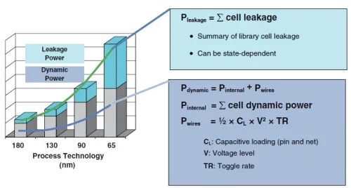
Dynamic Power and Static Power
IC design must consider both dynamic power and static power.
Dynamic power is consumed when transistors switch and depends on clock frequency and switching activity.
Static power is consumed due to transistor leakage current and is independent of clock frequency or switching activity.
Dynamic power consists of switching power and short-circuit power. Switching power is consumed when the load capacitance is charged and discharged. Short-circuit power is the current that flows between PMOS and NMOS during logic transitions. The following figure illustrates switching power:
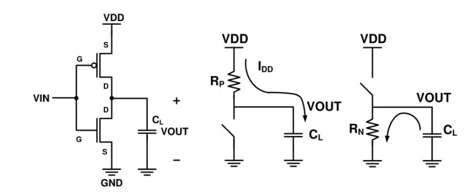
When an inverter output transitions from 0 to 1, the PMOS charges the load capacitance; when it transitions from 1 to 0, the NMOS discharges the load capacitance. Therefore, dynamic power is related to supply voltage, load capacitance, clock frequency, and switching activity.
In early CMOS technologies, leakage current was small. As transistor dimensions and threshold voltages decreased, leakage power increased and in some cases reached levels comparable to dynamic power. Transistors leak current whenever powered; slowing or stopping the clock does not reduce leakage. Only lowering or removing the supply voltage can reduce or eliminate leakage power.
Low-Power Design Techniques
Reducing power is a major goal in digital IC design. Strategies can be applied at the RTL and gate levels. Clock gating is a common method to stop the clock signal to registers when their state does not change, reducing dynamic power. Other methods, such as dynamic voltage and frequency scaling, can adjust voltage and frequency based on workload, but are more complex to implement.
As process technology advances, power issues become more prominent, requiring additional techniques to meet power budgets.
1. Lowering Supply Voltage
Reducing supply voltage is a fundamental way to lower power because power is proportional to the square of the supply voltage.
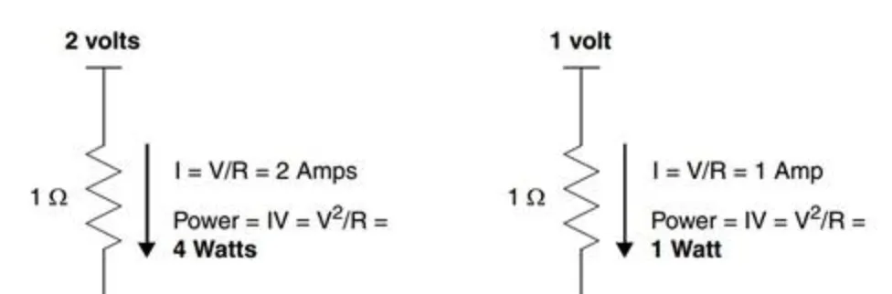
If supply voltage is reduced by 50%, power can drop by 75%. CMOS technology has progressively reduced supply voltages to lower power. From the 5 V bipolar TTL era in the 1980s to current advanced processes, supply voltages have fallen to around 1 V. However, lowering supply voltage affects switching speed and noise margin, and can increase leakage and interface complexity.
2. Clock Gating
Clock gating effectively reduces dynamic power by stopping the clock to registers that maintain the same logic value, thereby avoiding unnecessary switching. A typical implementation is shown below:
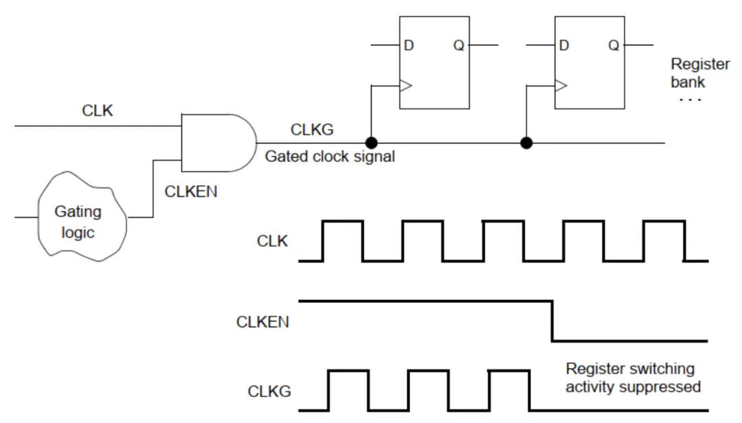
Clock gating is suitable for registers that must hold the same value over multiple clock cycles. Disabling the clock saves the power consumed by re-triggering the register each cycle. The main challenges are finding suitable insertion points and generating gate-enable signals at the right time. Clock gating is a mature technique and many synthesis tools can automatically insert clock-gating cells into the clock path. It is relatively simple to implement since it only requires netlist modification.
3. Multi-Threshold Standard Cell Libraries
Some standard cell libraries offer cells with different threshold voltages (Vt). The library can provide functionally identical cells implemented with low-Vt and high-Vt transistors.
- Low-Vt cells offer higher speed but higher leakage.
- High-Vt cells have lower leakage but slower speed.
Synthesis tools select appropriate cell types based on the trade-off between speed and power. For example, low-Vt cells can be used on critical paths and high-Vt cells on noncritical paths.
4. Multi-Voltage Design
Different parts of a chip may have different speed requirements. For example, a CPU or RAM may require higher speed than peripheral modules. Lower supply voltage reduces power but also reduces speed.
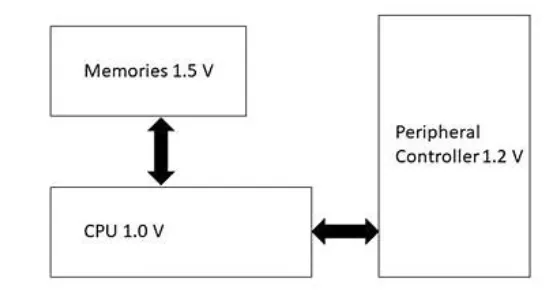
Providing two or more supply voltages on a single chip adds complexity. The power grid must route each voltage separately to the appropriate modules. If logic signals cross voltage domains, level shifters are required to produce signals with correct voltage swing. A level shifter needs power rails matching both input and output voltages. In the example above, a level shifter converts a 1.0 V signal to 1.5 V and requires supplies for both voltages.
5. Power Switching
Power switching disconnects power to parts of a chip that are not needed.
For example, in a mobile SoC, a voice-processing block can be powered down during standby and must be woken up when a call is made or received.
Power switching can significantly reduce total power by lowering both static and dynamic power, but it introduces challenges such as power control, power-switch networks, isolation cells, and retention registers.
Power control is the logic that decides when to turn power off and on. Power transitions incur time and energy overhead, so the controller must determine appropriate power-down intervals. Modules eligible for power-down connect to always-on rails through power-switch networks composed of series transistors.
When on, the switch connects the power rail to the module logic; when off, it disconnects the module from the power rail. High-Vt transistors implemented in MTCMOS are commonly used as power switches to minimize leakage; their switching speed is less critical. PMOS switches are placed between VDD and the module power pin, and NMOS between VSS and the module ground pin, as shown below.
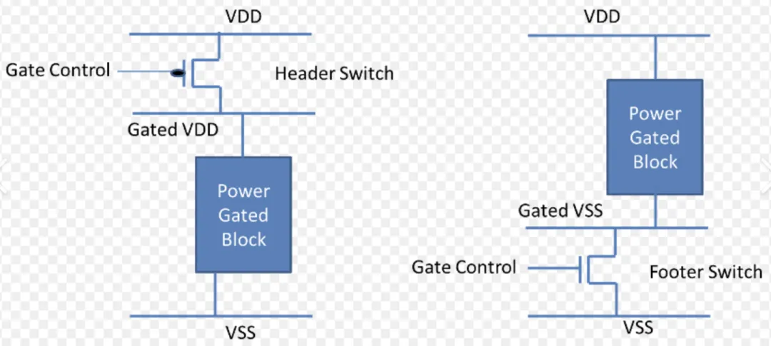
The number, drive strength, and placement of switches must be chosen to ensure acceptable IR drop when the module is active.
The coarse-grain strategy shown above shares one or more parallel power switches per module. In fine-grain strategies, each library cell has its own power switch, which can further reduce power but increases area.
When signals flow from a powered-down module to an always-on module, isolation cells are required. Isolation cells provide a fixed logic value to the always-on domain when the source domain is powered down, preventing unintended leakage. A simple isolation cell implementation is shown below.
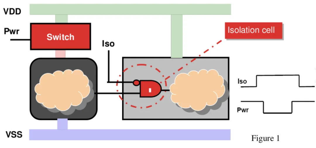
When the left module is powered on, the iso signal is low and the isolation cell passes the signal (with some delay). When the left module is powered down, iso is high and the isolation cell forces the output to a constant logic 0. Other isolation cells can force logic 1 or preserve the last value. Isolation cells require an always-on power supply.
Power switching can be combined with multi-voltage techniques: different modules may operate at different voltages and be powered down independently. In that case, interface cells must provide both level shifting and isolation; such cells are called enable level shifters and require two independent supplies like ordinary level shifters.
Restoring a module after power-up typically requires returning it to its pre-power-down state. One approach is to copy register contents to off-module RAM before power-down and restore them after power-up. Another approach uses retention registers inside the powered-down module. Before power-down, retention registers save data to shadow registers that remain powered during power-down. After power-up, data are restored from the shadow registers to the main registers. Shadow registers are powered by an always-on supply and use high-Vt transistors to minimize leakage, while main registers use low-Vt transistors for speed. A retention register implementation is shown below.
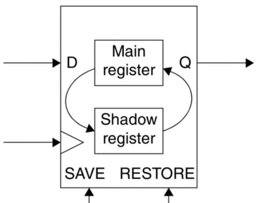
SAVE signals copy register data into shadow registers before power-down; RESTORE signals recover data after power-up. Retention registers use level-sensitive control signals. They occupy more area than normal registers and require an always-on power supply in addition to the module supply.
6. Dynamic Voltage and Frequency Scaling (DVFS)
Building on multi-voltage techniques, voltage and frequency can be adjusted dynamically according to runtime workload to optimize power. For example, a processor in a laptop can use lower voltage and frequency for light tasks to save power, and higher voltage and frequency for demanding tasks like 3-D rendering to improve performance.
Chip power supplies can provide multiple discrete or continuous voltage levels. DVFS requires multilevel supplies and control logic to determine the optimal voltage for a given task.
Designing, implementing, verifying, and testing DVFS is challenging due to the many possible voltage and frequency combinations.
DVFS can be combined with power switching: modules can operate at different voltages to meet performance requirements or be fully powered down when idle.