ALLPCB


Introduction
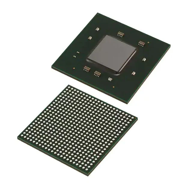
The semiconductor supply chain separates design and manufacturing. After logic and physical design are completed, design houses hand off results to wafer fabs. Fabs fabricate many identical chips on a single wafer. Individual dies are then singulated from the wafer. A die is a fragile piece of silicon and cannot be used directly; it requires an external protective enclosure, commonly referred to as a package. Packaging secures the die to a substrate and electrically connects the die pads to package pins or pads.
Wire Bonding
The most common traditional method is wire bonding. The die is mounted face up on a substrate and fine metal wires, typically gold or copper, connect die bond pads to substrate pads. The die, substrate, and wires are then encapsulated with plastic, ceramic, or other materials. Wire bonding is relatively simple and cost-effective, but it increases the final package footprint compared with the die and limits maximum I/O count.
Flip-Chip
Flip-chip technology attaches solder bumps to die pads before singulation. During assembly the die is flipped so the bumped side faces the carrier, and bumps are bonded to carrier pads using heat and pressure. Flip-chip supports higher I/O density, reduces package size closer to die dimensions, and improves electrical and thermal performance. However, as die functionality and I/O counts grow, routing many bumps within limited die area while meeting strict bump pitch becomes increasingly difficult.
Fan-Out WLP (FOWLP)
Fan-out wafer-level packaging (FOWLP) first singulates dies and places them face down on a carrier to form a reconstituted wafer. Redistribution layers (RDLs) are then fabricated to route connections outward from the die. FOWLP allows I/Os to be redistributed beyond the die outline, increasing package area relative to die (the "fan-out") and enabling higher I/O counts without using a traditional substrate.
Multi-Die Packaging: 2D, 2.5D, and 3D
Packaging multiple dies together can be implemented in several ways, commonly categorized as 2D, 2.5D, and 3D.
2D Multi-Die
The simplest approach mounts multiple dies face down on a common substrate; die-to-die interconnects rely on substrate wiring. The limitation is the relatively low wiring density of organic substrates, which constrains die-to-die bandwidth and routing complexity.
2.5D with Silicon Interposer
A higher-density solution adds a silicon interposer. Multiple face-down dies connect to the silicon interposer, and die-to-die interconnects are routed in the interposer. Because the interposer is fabricated with semiconductor processes, its wiring density is much higher than an organic substrate, alleviating die-to-die connectivity limits. Drawbacks include the large area of an interposer that must accommodate multiple dies and the higher cost and manufacturing difficulty of large-area silicon interposers. A leading example of this approach is TSMC's CoWoS.
Embedded Multi-Die Interconnect Bridge (EMIB)
To reduce the area and cost of a full silicon interposer, EMIB uses small silicon bridges embedded in the substrate to provide high-density die-to-die connections, while die-to-substrate connections use conventional methods. EMIB reduces silicon usage and relaxes some multi-die packaging constraints.
FOCoS
Fan-Out Chip on Substrate (FOCoS) implements chip fan-out on a substrate. Silicon bridges can be embedded within RDL layers. Depending on the sequence of RDL formation and chip placement, FOCoS is classified as chip-last or chip-first.
3D Packaging
3D packaging stacks dies vertically, with inter-die connections implemented through-through silicon vias (TSVs). Vertical stacking increases integration density but also raises complexity and cost. Fabricating many through-silicon vias in thin, fragile dies and assembling tall stacks pose significant manufacturing challenges. Note that some NAND flash stacking methods do not use TSVs and are not strictly 3D TSV-based packaging.
Variants and Industry Implementations
Various vendors have developed proprietary 3D and advanced multi-die packaging technologies, such as Intel Foveros, SoIC, and others. Each approach balances interconnect density, thermal and power considerations, manufacturability, and cost.
Analogy and Summary
As a conceptual analogy: 2D packaging is like a single-story building where each room is a functional block; 2.5D is like a compound of single-story houses arranged on a shared courtyard, with the courtyard acting as an interconnect layer; 3D packaging is like a multi-story building where vertical stairs or elevators provide inter-floor connections. Each packaging class offers trade-offs between integration density, performance, and manufacturing complexity.