 ALLPCB


When it comes to PCB assembly, achieving optimal solderability is a top priority for engineers and manufacturers. The combination of outer layer copper thickness and surface finish plays a critical role in ensuring reliable solder joints, preventing defects, and enhancing the overall performance of a printed circuit board (PCB). But how do you choose the right pairing of copper thickness and surface finish like ENIG or HASL to avoid solderability issues? In this comprehensive guide, we’ll break down the key factors, compare popular options, and provide actionable insights to help you make informed decisions for your PCB projects.
Whether you’re dealing with complex multilayer boards or simple single-layer designs, understanding the relationship between copper thickness and PCB surface finish is essential. Let’s dive into the details of how these elements impact solderability and what combinations work best for different applications.
Why Copper Thickness and Surface Finish Matter for Solderability
Solderability refers to how well solder adheres to the copper pads on a PCB during assembly. Poor solderability can lead to weak joints, cold solder defects, or even complete assembly failures. Two primary factors influence this process: the thickness of the outer layer copper and the type of surface finish applied to protect the copper and facilitate soldering.
Copper thickness determines the current-carrying capacity, heat dissipation, and mechanical strength of the traces and pads. Meanwhile, the surface finish acts as a protective layer that prevents oxidation of the copper while ensuring a clean, solder-friendly surface. Choosing the wrong combination can result in issues like uneven solder distribution, insufficient wetting, or long-term reliability problems.
Key Challenges in PCB Assembly
Solderability issues often arise from mismatches between copper thickness and surface finish. For instance, a thicker copper layer might require a more robust surface finish to handle higher heat during soldering, while a thinner layer might need a finish that ensures even solder spread. Common problems include:
- Insufficient wetting: Solder fails to spread evenly across the pad, leading to weak joints.
- Oxidation: Exposed or poorly protected copper can oxidize, making soldering difficult.
- Thermal stress: Thicker copper layers may retain more heat, affecting the performance of certain surface finishes.
By understanding these challenges, you can select the right combination to ensure smooth PCB assembly and long-term durability.
Understanding Outer Layer Copper Thickness
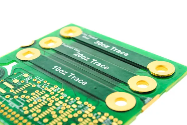
The outer layer copper thickness of a PCB typically ranges from 0.5 oz (17.5 microns) to 3 oz (105 microns) or more, depending on the application. This measurement refers to the weight of copper per square foot, which directly correlates to its thickness. Let’s explore how different copper thicknesses impact solderability and PCB performance.
Common Copper Thickness Options
- 0.5 oz (17.5 microns): Often used in low-power, lightweight designs like consumer electronics. Thin copper is easier to etch for fine traces but may struggle with heat dissipation during soldering.
- 1 oz (35 microns): A standard choice for most general-purpose PCBs. It offers a balance between current-carrying capacity and ease of soldering.
- 2 oz (70 microns): Suitable for high-current applications like power supplies. Thicker copper can handle more heat but may require adjustments in soldering temperature and time.
- 3 oz and above (105+ microns): Used in heavy-duty industrial or automotive applications. Soldering on such thick layers often requires specialized equipment to ensure proper heat distribution.
Impact on Solderability
Thicker copper layers tend to retain more heat during soldering, which can lead to uneven heating if not managed properly. For instance, a 2 oz copper layer might cause the solder to cool too slowly, resulting in grainy or brittle joints. On the other hand, thinner copper, such as 0.5 oz, may overheat quickly, risking damage to delicate components or the board itself.
The key is to match the copper thickness with the right soldering technique and surface finish. For thicker copper, preheating the board or using a finish with high thermal stability can prevent issues. For thinner copper, a finish that promotes quick and even solder wetting is ideal.
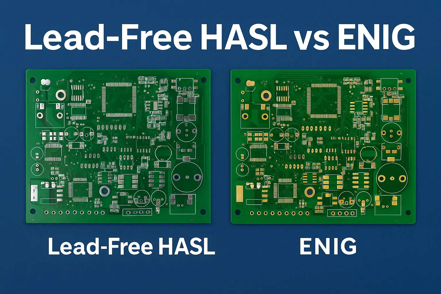
Exploring PCB Surface Finishes: ENIG vs. HASL
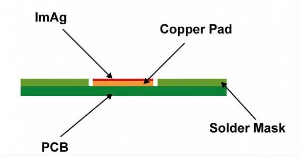
The surface finish on a PCB protects the exposed copper from oxidation and ensures a reliable surface for soldering. Two of the most popular finishes are Electroless Nickel Immersion Gold (ENIG) and Hot Air Solder Leveling (HASL). Each has unique properties that affect solderability, cost, and performance.
ENIG (Electroless Nickel Immersion Gold)
ENIG consists of a thin layer of gold over a nickel barrier, applied through a chemical process. It’s widely used for its excellent solderability and durability.
- Advantages:
- Flat, uniform surface ideal for fine-pitch components.
- Excellent resistance to oxidation, ensuring long shelf life.
- Compatible with a wide range of copper thicknesses, from 0.5 oz to 3 oz.
- Disadvantages:
- Higher cost compared to other finishes.
- Potential for "black pad" defects if the nickel layer is improperly applied, leading to solderability issues.
ENIG works well with various soldering processes, including reflow and wave soldering. Its gold layer, typically 2-5 microinches thick, ensures good wetting, while the nickel layer (150-250 microinches) acts as a robust barrier against copper diffusion.
HASL (Hot Air Solder Leveling)
HASL involves dipping the PCB in molten solder and using hot air to level the coating. It’s a cost-effective option often used in simpler designs.
- Advantages:
- Low cost and widely available.
- Good solderability for through-hole components and larger pads.
- Suitable for copper thicknesses of 1 oz to 2 oz in most cases.
- Disadvantages:
- Uneven surface, making it less ideal for fine-pitch or surface-mount components.
- Poorer shelf life due to potential oxidation of the solder coating.
HASL typically results in a solder layer of 1-25 microns thick, which can vary across the board. This inconsistency can cause solderability issues with thinner copper layers or high-density designs.
How Copper Thickness and Surface Finish Interact
The interaction between copper thickness and surface finish directly affects solderability during PCB assembly. Let’s look at some specific combinations and their outcomes.
Thin Copper (0.5 oz) with ENIG
For lightweight designs with thin copper, ENIG provides a flat, reliable surface that ensures even solder distribution. The thin copper heats up quickly, and ENIG’s gold layer promotes excellent wetting, reducing the risk of cold solder joints. This combination is ideal for high-density boards with fine-pitch components, such as those in mobile devices.
Standard Copper (1 oz) with HASL
A 1 oz copper layer paired with HASL is a common choice for general-purpose PCBs. The moderate thickness handles typical current loads, while HASL offers a cost-effective finish with decent solderability for through-hole and larger SMT components. However, care must be taken to avoid uneven solder distribution due to HASL’s inconsistent surface.
Thick Copper (2-3 oz) with ENIG
For high-current applications, thicker copper layers benefit from ENIG’s thermal stability and uniform coating. The nickel layer in ENIG withstands the prolonged heat exposure often required when soldering thick copper, ensuring reliable joints. This combination is often used in power electronics and industrial equipment.
Thick Copper (2-3 oz) with HASL
While HASL can be used with thicker copper, it’s less ideal due to its uneven surface and lower thermal resistance. The combination might work for simpler designs with through-hole components, but it risks solderability issues in high-density or fine-pitch applications.
Common Solderability Issues and Solutions
Even with careful selection, solderability issues can still occur. Here are some frequent problems and how to address them based on copper thickness and surface finish choices.
Insufficient Wetting
This happens when solder doesn’t spread evenly across the pad. It’s often seen with HASL on thinner copper layers due to surface inconsistencies. Switching to ENIG or ensuring proper flux application during soldering can improve wetting. For thicker copper, preheating the board helps achieve uniform heat distribution.
Oxidation of Copper
Oxidation is a risk if the surface finish fails to protect the copper, especially with HASL after prolonged storage. ENIG offers better resistance to oxidation, making it a safer choice for boards that may sit on the shelf before assembly. Storing PCBs in a controlled, low-humidity environment also helps.
Thermal Stress During Soldering
Thicker copper layers retain more heat, which can stress the surface finish or components. Using ENIG with its robust nickel barrier minimizes this risk. Adjusting the soldering profile, such as increasing preheat time, can also prevent thermal shock.
Tips for Choosing the Right Combination
Selecting the optimal copper thickness and surface finish for your PCB project requires balancing performance, cost, and manufacturability. Here are some practical tips to guide your decision:
- Consider the application: High-current designs need thicker copper (2-3 oz) and a durable finish like ENIG. Low-power, compact designs can use thinner copper (0.5-1 oz) with either ENIG or HASL.
- Evaluate component types: Fine-pitch or surface-mount components benefit from ENIG’s flat surface, while through-hole components can work well with HASL.
- Factor in cost: HASL is more budget-friendly for simpler projects, while ENIG justifies its higher cost in high-reliability or complex designs.
- Test before production: Run small batches with your chosen combination to identify potential solderability issues before full-scale manufacturing.
Conclusion: Achieving Optimal Solderability in PCB Assembly
The right combination of outer layer copper thickness and PCB surface finish is crucial for ensuring optimal solderability and reliable performance in PCB assembly. Whether you choose ENIG for its uniform surface and durability or HASL for its affordability, pairing it with the appropriate copper thickness—be it 0.5 oz for lightweight designs or 3 oz for high-current applications—can make all the difference in avoiding solderability issues.
By carefully considering the demands of your project, from component types to environmental conditions, you can select a combination that enhances assembly quality and long-term reliability. Armed with this knowledge, you’re better equipped to tackle the challenges of PCB design and manufacturing with confidence.
At ALLPCB, we’re committed to supporting your success with high-quality manufacturing solutions tailored to your specific needs. Explore our range of options for copper thickness and surface finishes to bring your next project to life with precision and reliability.


