 ALLPCB


In the world of electronics manufacturing, mixed technology PCB assembly, which combines Surface Mount Technology (SMT) and Through-Hole (PTH or THT) components, is a powerful approach for creating high-performance, reliable, and cost-effective circuit boards. If you're searching for SMT PTH assembly best practices, mixed technology PCB design rules, or ways to optimize mixed technology PCB cost, you're in the right place. This guide will walk you through the essentials of integrating SMT and PTH technologies, offering practical tips and strategies to streamline your design and assembly process.
At its core, optimizing mixed technology PCB assembly involves balancing the precision and compactness of SMT with the durability and power-handling capabilities of PTH. By following best practices in design, component selection, and manufacturing, you can achieve efficient production while minimizing costs and errors. Let’s dive into the details of how to make this integration seamless and effective.
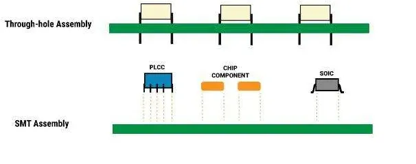
What Is Mixed Technology PCB Assembly?
Mixed technology PCB assembly refers to the process of building circuit boards that use both SMT and PTH components. SMT components are mounted directly onto the surface of the PCB, allowing for smaller, lighter designs with high-speed performance. PTH components, on the other hand, are inserted into drilled holes and soldered on the opposite side, providing greater mechanical strength and reliability for high-power or heavy components.
This hybrid approach is common in applications like power supplies, industrial equipment, and IoT devices, where a combination of compact, high-density circuits and robust connectors or capacitors is needed. Understanding how to integrate these technologies effectively is key to achieving a balance between performance, reliability, and cost.
Benefits of Mixed Technology PCB Assembly
Using a mix of SMT and PTH offers several advantages for designers and manufacturers. Here are some key benefits:
- Enhanced Flexibility: Mixed technology allows you to choose the best components for each part of your design, whether they are available in SMT for compact layouts or PTH for durability.
- Improved Reliability: PTH components provide strong mechanical bonds, ideal for connectors or components under stress, while SMT ensures precision in high-density areas.
- Cost Efficiency: By strategically using SMT for smaller, cheaper components and PTH only where necessary, you can reduce overall material and assembly costs.
- Performance Optimization: SMT supports high-speed signal transmission (often exceeding 1 GHz in modern designs), while PTH handles higher current loads (up to 10A or more in some cases), making this combination ideal for complex systems.
SMT PTH Assembly Best Practices
To ensure a smooth assembly process for mixed technology PCBs, follow these best practices. These guidelines focus on preparation, execution, and quality control to minimize errors and improve efficiency.
1. Plan Component Placement Carefully
Component placement is critical in mixed technology designs. Place SMT components on one side of the board (or both, if needed) to maximize automation during assembly. Reserve PTH components for areas where mechanical strength or high power is required, such as connectors or large capacitors. Keep a clearance of at least 2.5 mm between SMT and PTH components to avoid interference during soldering processes like wave soldering for PTH parts.
Additionally, group SMT components together to streamline the pick-and-place process, and ensure PTH components are aligned to minimize manual insertion time. Proper planning reduces assembly errors and speeds up production.
2. Optimize Soldering Processes
Mixed technology assembly often requires multiple soldering steps. Typically, SMT components are soldered first using reflow soldering, followed by PTH components using wave soldering or manual soldering. To avoid thermal stress on components, ensure the reflow temperature profile stays within safe limits (usually 220-260°C for lead-free solder) and limit exposure time to prevent damage to sensitive SMT parts.
For PTH soldering, use wave soldering only if the board design allows it, as this method can be faster for high-volume production. However, be cautious of SMT components on the bottom side, as they may require masking to prevent solder splash.
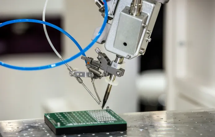
3. Use Automated and Manual Assembly Strategically
SMT assembly benefits greatly from automation, with pick-and-place machines achieving placement rates of up to 100,000 components per hour in high-end setups. Use this to your advantage for SMT parts. For PTH components, which often require manual insertion, limit their use to essential areas to reduce labor costs and time. If manual assembly is unavoidable, ensure clear documentation and training for workers to maintain consistency.
4. Conduct Thorough Testing and Inspection
Quality control is vital in mixed technology assembly. Use Automated Optical Inspection (AOI) for SMT components to detect misalignment or solder defects at a resolution as fine as 0.01 mm. For PTH components, X-ray inspection can verify solder joint integrity beneath the board. Testing should also include functional checks to ensure signal integrity (e.g., maintaining impedance within ±10% of design specs) and power handling capabilities.
Mixed Technology PCB Design Rules
Designing a mixed technology PCB requires adherence to specific rules to ensure manufacturability and performance. These design rules address layout, spacing, and thermal management to prevent issues during assembly and operation.
1. Maintain Proper Spacing and Clearances
Spacing is crucial to avoid interference between components and ensure soldering accuracy. Follow these guidelines:
- Keep a minimum of 0.2 mm spacing between SMT pads to prevent solder bridging.
- Ensure at least 1.5 mm clearance around PTH drill holes to accommodate soldering equipment and prevent thermal overlap with nearby SMT parts.
- Maintain a 3 mm edge clearance from the board’s edge for both SMT and PTH components to avoid damage during handling or assembly.
2. Design for Thermal Management
Mixed technology PCBs often combine high-power PTH components with densely packed SMT parts, leading to heat buildup. Use thermal vias (with a diameter of 0.3-0.5 mm) under high-power components to dissipate heat to internal copper layers. Additionally, place heat-generating components away from sensitive SMT parts, and consider adding heat sinks if power dissipation exceeds 2W per component.
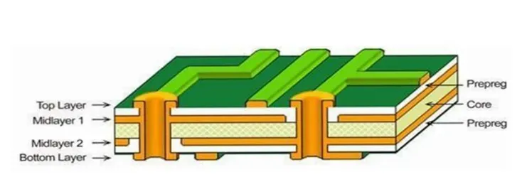
3. Optimize Layer Stackup
For mixed technology designs, a 4-layer or 6-layer PCB stackup is often ideal. Dedicate inner layers to ground and power planes to reduce noise and improve signal integrity for SMT circuits operating at high frequencies (e.g., 500 MHz or above). Ensure PTH components have access to these planes through properly sized vias to handle current loads without excessive voltage drop (aim for less than 0.1V drop across connections).
4. Minimize Via Usage for PTH Components
While vias are necessary for routing, excessive use near PTH components can weaken the board’s structure. Limit vias to 1-2 per PTH pad and ensure they are placed at least 0.5 mm away from the pad edge to avoid compromising mechanical strength.
Optimizing Mixed Technology PCB Cost
Cost optimization is a top priority for many engineers and manufacturers. By focusing on design efficiency, component selection, and assembly processes, you can significantly reduce expenses without sacrificing quality. Here are actionable strategies to achieve this.
1. Prioritize SMT Where Possible
SMT components are generally cheaper and faster to assemble than PTH parts due to automation. For example, a typical SMT resistor might cost $0.01 per unit, while a comparable PTH resistor could cost $0.05 or more due to manual labor. Use SMT for low-power, high-density areas, reserving PTH for components like large transformers or connectors that require mechanical strength.
2. Standardize Components
Reduce costs by standardizing component packages and values across your design. For instance, using a single type of 0805 SMT resistor in multiple values rather than mixing 0603 and 1206 packages simplifies procurement and assembly setup, potentially saving up to 10-15% on component costs in bulk orders.
3. Minimize Board Size and Layer Count
Smaller boards and fewer layers directly lower material and manufacturing costs. Optimize your layout to fit within a compact footprint while maintaining clearances. A 4-layer board might cost $0.50 per square inch, while a 6-layer board could jump to $0.80 per square inch. Use design software to simulate layouts and find the smallest possible size without compromising performance.
4. Partner with a Reliable Manufacturing Service
Choosing a manufacturing partner with expertise in mixed technology assembly can save costs in the long run. Look for services that offer Design for Manufacturability (DFM) feedback to catch potential issues early, reducing the need for costly revisions. Efficient assembly processes and bulk purchasing power can also lower per-unit costs by 5-20% for large production runs.
Common Challenges in Mixed Technology PCB Assembly and How to Overcome Them
While mixed technology offers many benefits, it also comes with unique challenges. Here’s how to address some common issues:
- Thermal Stress During Soldering: Multiple soldering cycles can stress components. Use low-temperature solder paste for SMT (melting point around 180°C) if a second wave soldering step is needed for PTH parts.
- Component Misalignment: Ensure precise fiducial markers (at least 1 mm in diameter) are included in the PCB design for accurate machine alignment during SMT placement.
- Assembly Delays: Mixing automated and manual processes can slow production. Streamline workflows by completing SMT assembly first and organizing PTH insertion as a separate, efficient step.
Conclusion
Optimizing mixed technology PCB assembly is all about striking the right balance between SMT and PTH integration. By following SMT PTH assembly best practices, adhering to mixed technology PCB design rules, and focusing on optimizing mixed technology PCB cost, you can create reliable, high-performance boards that meet your project’s needs without breaking the budget.
Start with careful planning of component placement and soldering processes, design with manufacturability in mind, and prioritize cost-saving strategies like standardization and SMT usage. With these steps, you’ll be well-equipped to tackle the challenges of mixed technology assembly and achieve efficient, high-quality results. Whether you’re working on a small prototype or a large-scale production run, these guidelines will help you succeed in the complex world of PCB manufacturing.


