ALLPCB


Overview
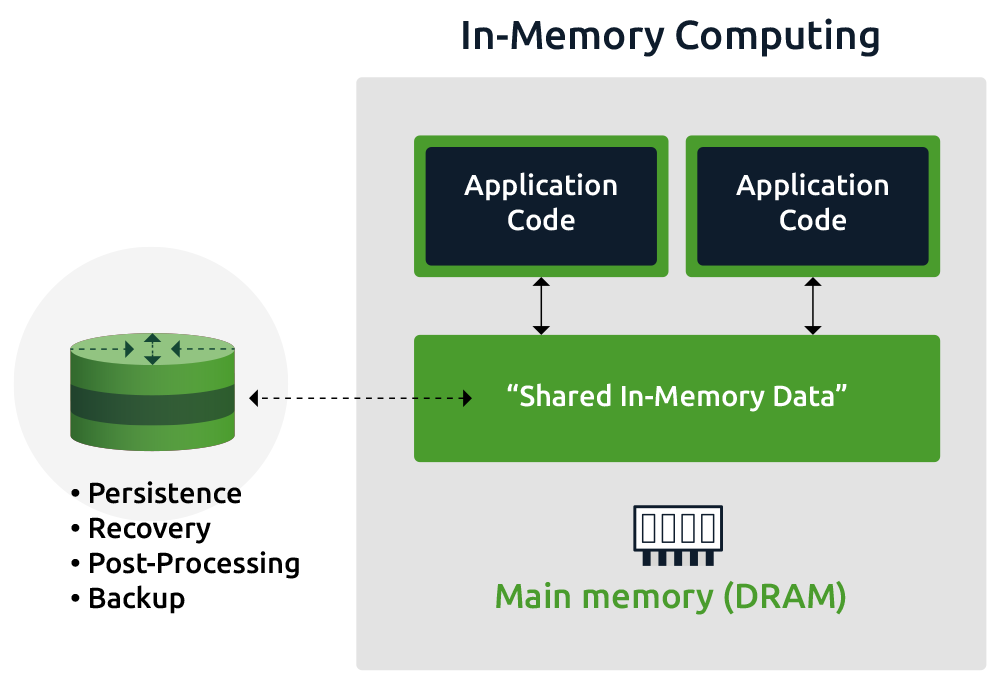
With the rapid growth of digital data, demands for processing and storage are increasing. The traditional separation of compute and memory is becoming less able to meet requirements for high efficiency and low power consumption. Memory-compute integration (sometimes called compute-in-memory or processing-in-memory) is one approach attracting significant attention as a way to address these challenges.
1. Advantages of memory-compute integration
Memory-compute integration helps mitigate the "memory wall" and the "power wall" associated with the von Neumann architecture. The von Neumann model requires frequent data transfers between memory cells and processing units. These transfers consume substantial energy. Intel's research indicates that at the 7 nm node, data movement energy can reach about 35 pJ/bit, accounting for roughly 63.7% of total power. Increasing losses from data transfers constrain chip performance and efficiency, forming a "power wall."
The "memory wall" refers to the gap between memory performance and CPU performance: processors often spend considerable time waiting for memory read/write operations, reducing overall system performance. This is especially problematic for workloads like deep learning, where frequent data movement between compute and storage dominates performance and energy consumption.
Memory-compute integration reduces unnecessary data movement latency and energy by performing computation closer to or inside memory cells. By leveraging storage elements for computation, it can multiply effective compute throughput by orders of magnitude while reducing system cost and energy consumption.
As a non–von Neumann architecture, memory-compute integration can offer very high peak compute (above 1000 TOPS) and much-improved efficiency (on the order of 10–100 TOPS/W) in targeted domains, outperforming many current ASIC designs. Besides AI workloads, memory-compute approaches are applicable to sensing-compute integrated chips and neuromorphic processors, positioning them as a key architecture for future big-data compute chips.
2. Classification of memory-compute technologies
There is not yet a single universally accepted classification for memory-compute technologies. A common approach is to categorize them by the physical proximity between compute and storage: near-memory computing (PNM), processing-in-memory (PIM), and compute-in-memory (CIM).
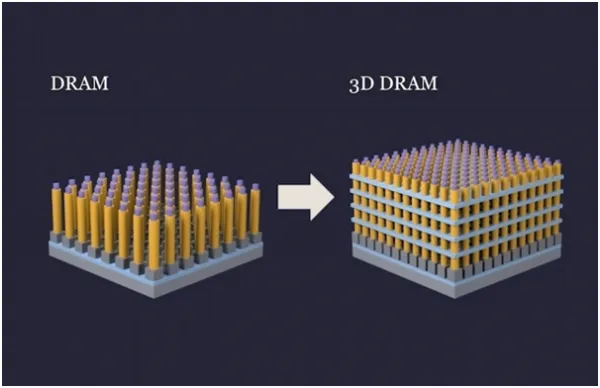
Near-memory computing (PNM) is a relatively mature path. It uses advanced packaging to place compute logic and memory close together, reducing the path length between them to achieve high I/O density, increased memory bandwidth, and lower access overhead. PNM implementations often use 2.5D or 3D stacking and are widely used in CPU and GPU systems.
Processing-in-memory (PIM) emphasizes embedding computation as deeply as possible within the memory subsystem. By reducing the frequency of processor accesses to memory—because many operations are executed inside the memory—PIM designs alleviate the von Neumann bottleneck and improve throughput and energy efficiency.
Compute-in-memory (CIM) merges computation and storage in the same elements. Two main approaches exist. The first modifies memory circuits so the memory itself performs computation during readout or in decoder stages; this is commonly applied to SRAM or MRAM arrays and can achieve high energy efficiency, although numerical precision may be limited. The second approach integrates additional compute units within the memory die to support higher-precision operations; this is often targeted at DRAM-like memories, but integrating logic with DRAM processes presents substantial challenges.
Compute-in-memory describes the approach many startups in China refer to as memory-compute integration.
Different companies have chosen distinct technical tracks: some focus on optimizing memory-compute co-design for large-scale data processing, while others prioritize architectural flexibility and scalability. The choice of storage medium also varies: volatile memories such as SRAM and DRAM and nonvolatile memories such as Flash or MRAM each bring their own trade-offs.
3. Industry activity and vendor approaches
Since around 2017, major firms such as NVIDIA, Microsoft, and Samsung proposed memory-compute prototypes, and startups in China began developing memory-compute chips. Large vendors often prioritize solutions that are practical and deployable in the near term; as a result, near-memory computing has become a favored approach. Companies with broad ecosystems, as well as established chip vendors such as Intel and IBM, have investments in near-memory compute.
International vendors
Samsung has explored multiple paths. In early 2021, Samsung announced an HBM-based memory integrating an AI processor capable of around 1.2 TFLOPS, embedding AI engines into each memory vault so some processing is moved into HBM. Samsung reported that this HBM-PIM approach can improve system performance while significantly reducing energy for certain workloads.
In 2022, Samsung published research in Nature demonstrating a compute-in-memory implementation based on MRAM. The team built a 28 nm CMOS MRAM array and ran tasks such as handwritten digit recognition and face detection, reporting recognition accuracies of approximately 98% and 93%, respectively.
SK Hynix announced PIM research in 2022 and developed a sample called GDDR6-AiM that adds compute capabilities to GDDR6 memory operating at 16 Gbps. SK Hynix reported that systems combining GDDR6-AiM with CPU/GPU can achieve significant speedups for specific workloads. Later in 2022, SK Hynix announced a CXL-based computational memory solution (CMS).
TSMC researchers presented a digital-enhanced SRAM design for in-memory computing at ISSCC 2021 aimed at supporting larger neural networks. In January 2024, TSMC and ITRI reported an SOT-MRAM array chip with fast operation (around 10 ns) and claimed significantly lower power compared with comparable STT-MRAM implementations, indicating progress in next-generation MRAM technology.
Intel has been active in MRAM development, introducing STT-MRAM research results based on a 22 nm FinFET process in 2018 and positioning MRAM as a key nonvolatile memory technology for integration with logic processes.
3. Toward large-scale deployment
Growing AI compute demand has pushed memory-compute technologies closer to mass production. As maturity and commercial deployments increase, the addressable market could expand rapidly.
Market research cited in 2023 forecast that the global memory-compute technology market could reach approximately USD 30.63 billion by 2029, with a very high compound annual growth rate projected over the coming years. This growth projection reflects broad applicability across data processing, AI, and IoT domains.
Despite the potential, memory-compute integration faces technical and ecosystem challenges: the field requires complex system-level innovation, supply-chain and process support vary across storage media and technologies, and downstream application integration is still evolving. These challenges also represent areas where comprehensive technical barriers can be established as the industry consolidates.
As memory-compute technologies progress and find broader application, they are expected to play an increasingly important role across many sectors and to influence the evolution of related technology stacks and supply chains.