ALLPCB


IGBT structure and gate-drive behavior
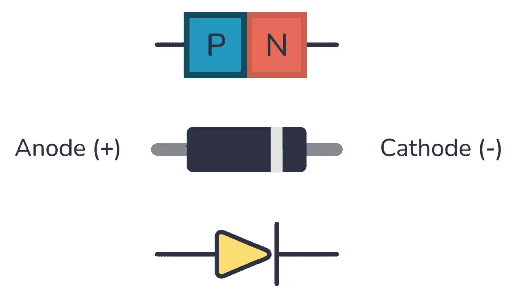
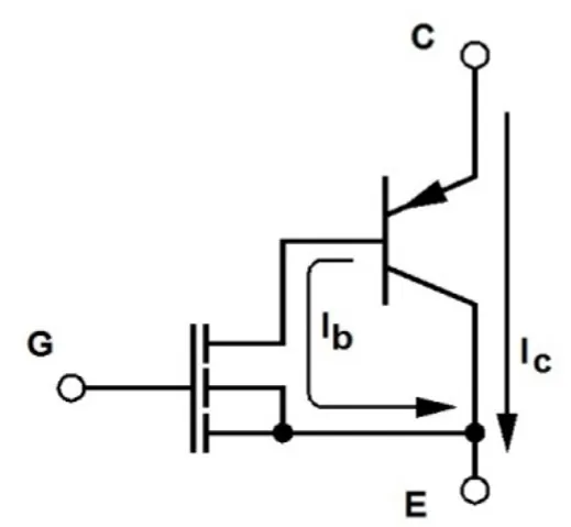
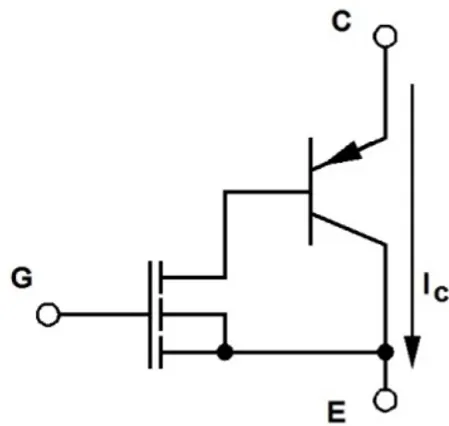
An IGBT combines properties of MOSFETs and bipolar junction transistors and has three terminals: gate, collector, and emitter. From the perspective of gate drive, its behavior is similar to a MOSFET, while its current path is similar to the collector-emitter path of a BJT.
Turn-on and turn-off currents
To turn the BJT portion on and off quickly, the gate must be driven with sufficient current in both directions to move carriers into and out of the base region. When the gate is driven high, a low-impedance path exists from the bipolar transistor base to emitter, which enables rapid conduction. The higher the gate drive level, the faster collector current begins to flow. The base and collector currents during turn-on are illustrated below.
Turn-off is different. When the gate is pulled low, there is no current path for base current in the BJT, which initiates turn-off. However, to achieve fast turn-off, current must be forced out of the base terminal. Because there is no mechanism to instantly remove stored carriers from the base, BJT turn-off is relatively slow, producing a tail current while stored charge is swept out by emitter current. The turn-off waveform is shown below.
Switching speed, dv/dt, and topology choices
Faster gate drive dv/dt (resulting from higher gate drive current capability) will switch an IGBT on and off more quickly, but the device has intrinsic limits, particularly on turn-off speed. Because of these limits, switching frequencies are commonly in the 20 kHz to 50 kHz range, although higher or lower frequencies are used in special cases. IGBTs are typically used in high-power circuits (Po > 1 kW) such as resonant and hard-switching topologies. Resonant topologies minimize switching loss by operating in either zero-voltage or zero-current switching modes.
Slower dv/dt can improve EMI performance and reduce spike formation during switching transitions, at the cost of increased switching time and higher switching losses.
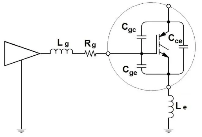
Miller-induced secondary turn-on and parasitic capacitances
MOSFETs can experience secondary turn-on due to very high dv/dt on the drain, sometimes in the range of 1000–10000 V/us. Although IGBT switching is usually slower than MOSFET switching, high voltages can still produce significant dv/dt levels. If the gate resistor is too large, the device may experience secondary turn-on.
When the driver pulls the gate low during turn-off, collector voltage rises. Due to the capacitive divider formed by Cgc and Cge, this collector voltage rise can inject voltage onto the gate. With a high gate resistance, the gate voltage can rise enough to re-enable conduction, causing large power pulses that may lead to overheating or device failure.
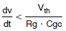
Limiting condition and definitions
The limiting relationship for avoiding secondary turn-on is shown below.
Definitions:
- dv/dt: rate of rise of the collector voltage during turn-off
- Vplateau: gate plateau voltage
- Rg: total gate resistance
- Cgc: gate-collector capacitance (Miller capacitance)
Note: datasheet Ciss is the series-parallel equivalent of Cge and Cgc. Similarly, Rg is the sum of driver output impedance, any physical gate resistor, and the internal gate resistance. Internal gate resistance can sometimes be estimated from the datasheet. If not available, measure with an LCR meter by shorting collector-emitter and measuring the equivalent series RC near the switching frequency. If the driver has a FET output stage, its impedance may be listed in the datasheet or approximated from peak drive current at the rated VCC level.
Maximum total gate resistance
The maximum total gate resistance is:

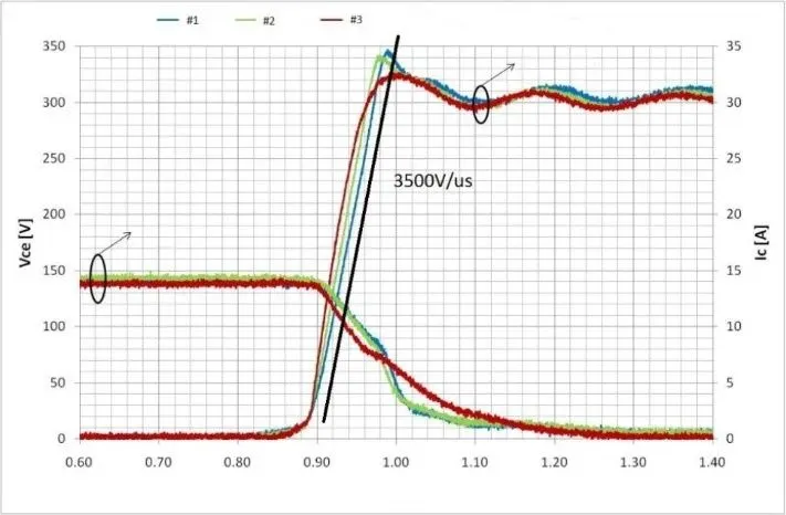
Maximum dv/dt depends on gate drive current and the impedance of the circuit around the IGBT. If a high-value resistor is used on the gate, validate the design on the actual circuit. The following turn-off waveforms were measured for three different IGBTs in the same motor-control circuit; the measured dv/dt in that application was 3500 V/s.
For this case, IGBT #2 has a typical Cgc of 84 pF and a gate threshold (plateau) of 7.5 V at 15 A. Using the formula above, the maximum total gate resistance for the circuit is:
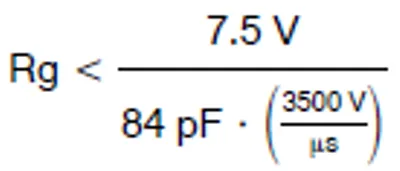
Rg < 25.5 ohm.
Thus, if the internal gate resistance is 2 ohm and the driver impedance is 5 ohm, the absolute maximum external gate resistor is 18 ohm. In practice, because of variations in IGBT, driver, board impedance, and temperature, a smaller maximum is recommended (for example, 12 ohm).
Related Reading: IGBT Switching Process and Driver Design Factors
Gate-drive circuit resonance and layout considerations
Removing the external gate resistor can improve high-frequency performance, provided it does not cause secondary turn-on. In some cases this works, but it can also cause oscillation due to impedance in the gate drive circuit.
The gate-drive circuit is effectively a series RLC resonant circuit. The capacitance comes mainly from IGBT parasitic capacitances; the inductances come from a combination of board trace inductance and bond wire inductance of both the IGBT and the driver.
With very low or no gate resistance, the resonant circuit may oscillate and produce high losses in the IGBT. A sufficiently large gate resistor is then required to damp the resonance and eliminate oscillation.
Because inductance is difficult to measure, calculating the appropriate damping resistor is challenging. The best way to minimize the required minimum gate resistance is to use good PCB layout practices.
- Keep the path between the driver and the IGBT gate as short as possible. This applies to the entire gate-drive path and the ground return path.
- If the controller does not include an integrated driver, place the IGBT driver close to the IGBT gate rather than routing the driver's input from the controller PWM output across the board. The current from controller to driver is small, so stray capacitance there has much less impact than the high-current, high-di/dt path from driver to IGBT.
- Use short, wide traces to minimize inductance.
Typical minimum gate resistance values (including driver impedance, external resistor, and internal IGBT resistance) are in the 2 ohm to 5 ohm range. After designing the board layout, determine and optimize the gate resistor value experimentally.
Related Reading: Comparison of SiC MOSFET, SJ-MOSFET and IGBT Performance
Design guidance
This article provides guidelines for maximum and minimum gate resistor values. The allowable range between these limits can be used to tune the circuit for maximum efficiency, minimum EMI, or other important parameters. Selecting a safe value between the extremes helps ensure robust operation.