ALLPCB


In the fast-paced world of PCB manufacturing, ensuring top-notch quality is a must. Integrating Automated Optical Inspection (AOI) with In-Circuit Testing (ICT) test fixtures offers a powerful solution to achieve enhanced quality control. This combination helps detect defects early, improves solder paste verification, and provides automated test solutions that are both cost-effective and efficient for debugging. In this blog, we’ll dive deep into how these technologies work together to boost PCB reliability and streamline production processes.
What Is Automated Optical Inspection (AOI) and ICT Testing?
Before exploring their integration, let’s break down the basics of AOI and ICT testing. AOI uses high-resolution cameras and advanced software to visually inspect PCBs for defects like misaligned components, missing parts, or poor solder joints. It’s a non-contact method that excels at spotting surface-level issues during manufacturing.
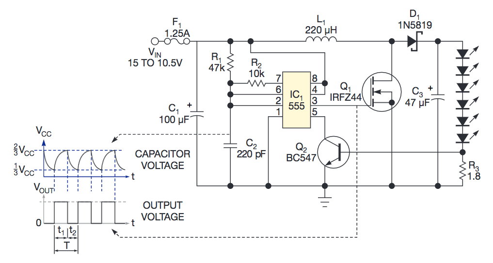
On the other hand, ICT testing involves using test fixtures to physically connect to a PCB and check for electrical functionality. It verifies component placement, polarity, and circuit integrity by sending electrical signals through predefined test points. Together, AOI and ICT cover both visual and functional aspects of quality control, making them a dynamic duo in PCB production.
Why Integrate AOI with ICT Test Fixtures?
The integration of AOI and ICT test fixtures creates a comprehensive quality control system. AOI catches visible defects early in the process, reducing the number of faulty boards that reach the ICT stage. Meanwhile, ICT ensures that the electrical performance meets design specifications, identifying issues that AOI can’t detect, such as open circuits or incorrect component values. This combined approach minimizes rework, cuts costs, and speeds up production timelines.

The Role of Solder Paste Verification in PCB Quality
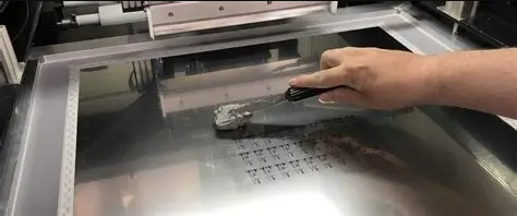
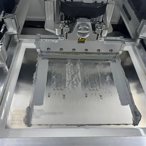
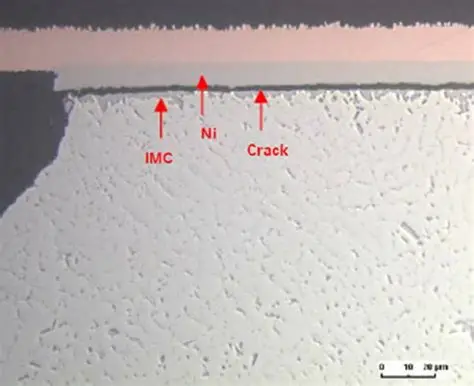
Solder paste verification is a critical step in PCB assembly, as improper solder application can lead to weak joints, shorts, or component failures. AOI plays a vital role here by inspecting solder paste deposits before components are placed. Using 2D or 3D imaging, AOI systems measure the height, volume, and alignment of solder paste to ensure it meets strict tolerances—often within 10-20 micrometers for high-density boards.
By catching solder paste issues early, manufacturers avoid costly rework after component placement. When paired with ICT, which tests the electrical integrity of solder joints post-assembly, this process ensures both the physical and functional quality of connections. This dual verification is especially important for complex boards with fine-pitch components, where even a slight deviation can cause failures.
Benefits of Automated Solder Paste Verification
- Precision: AOI systems detect deviations in solder paste volume as small as 5%, preventing potential defects.
- Speed: Automated inspection can scan a board in under 10 seconds, far faster than manual methods.
- Cost Savings: Early defect detection reduces scrap rates by up to 30%, based on industry studies.

Automated Test Solutions for Streamlined Production
Automation is the backbone of modern PCB manufacturing, and integrating AOI with ICT test fixtures offers robust automated test solutions. AOI systems quickly scan boards for visual defects at a rate of hundreds of units per hour, while ICT fixtures automatically test electrical parameters like resistance (down to 0.1 ohms) and capacitance (within 1% tolerance) without human intervention.
This synergy allows manufacturers to handle high-volume production while maintaining strict quality standards. Automated test solutions also reduce human error, as manual testing can miss subtle defects or introduce inconsistencies. By combining visual and electrical testing in an automated workflow, production lines achieve higher throughput—often increasing output by 20-40% compared to non-integrated systems.
Key Features of Automated Test Solutions
- Consistency: Automated systems perform the same checks repeatedly with zero deviation.
- Data Logging: Both AOI and ICT systems store inspection data for traceability, enabling quick identification of recurring issues.
- Scalability: These solutions adapt to different board designs with minimal reprogramming, supporting diverse product lines.
Cost-Effective Quality Control with AOI and ICT Integration
One of the standout benefits of integrating AOI with ICT test fixtures is the cost-effective approach to quality control. While the initial investment in AOI equipment and ICT fixtures can be significant—often ranging from $50,000 to $200,000 depending on complexity—the long-term savings are substantial. By detecting defects early, AOI reduces the number of boards that require costly ICT testing or rework, saving up to 25% on testing expenses per batch.
Moreover, ICT fixtures can be reused across multiple projects with minor adjustments, lowering per-unit testing costs. For high-volume runs, this integration cuts overall defect rates by as much as 50%, reducing scrap and warranty claims. For small to medium batches, the ability to quickly switch between AOI setups and ICT test programs ensures flexibility without sacrificing affordability.
Cost-Saving Strategies
- Early Detection: AOI identifies up to 90% of visible defects before ICT, minimizing expensive downstream fixes.
- Reduced Labor: Automation cuts manual inspection time by 70%, freeing up skilled workers for other tasks.
- Lower Failure Rates: Integrated systems achieve first-pass yield rates above 95%, reducing material waste.
Efficient Debugging with Integrated Systems
Debugging is a critical part of PCB manufacturing, and integrating AOI with ICT test fixtures makes it more efficient. AOI systems provide detailed visual data, pinpointing the exact location of defects like misaligned components or insufficient solder. For instance, AOI can detect a component offset by as little as 0.1mm, allowing technicians to address issues before they escalate.
ICT complements this by identifying functional failures, such as a resistor with a value outside the expected range (e.g., 1kΩ ±5%). By combining AOI’s visual feedback with ICT’s electrical diagnostics, manufacturers can trace defects to their root cause faster—often reducing debugging time by 40%. This is especially valuable for complex boards with hundreds of components, where manual debugging could take hours or even days.
Steps for Efficient Debugging
- Visual Inspection with AOI: Use AOI to identify surface defects and generate a defect map.
- Electrical Testing with ICT: Run ICT to confirm functional issues and correlate them with AOI findings.
- Data Analysis: Overlay AOI and ICT data to isolate root causes, such as a misaligned pad causing an open circuit.
- Corrective Action: Adjust assembly parameters or replace faulty components based on combined insights.

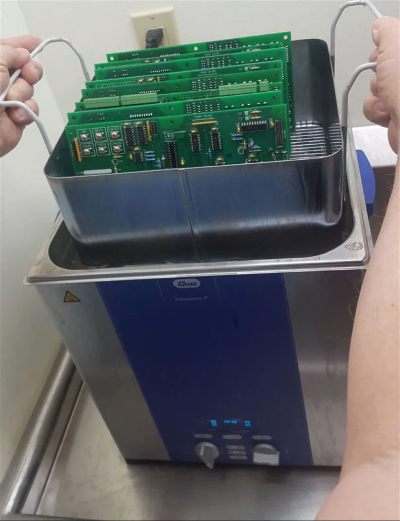
Challenges and Solutions in AOI and ICT Integration
While the benefits are clear, integrating AOI with ICT test fixtures comes with challenges. One common issue is aligning data from both systems, as AOI focuses on visual defects while ICT deals with electrical performance. Mismatched defect classifications can lead to confusion during debugging. To address this, manufacturers can use unified software platforms that integrate data from both systems, providing a single interface for analysis.
Another challenge is the upfront cost, especially for smaller manufacturers. However, modular AOI and ICT systems allow for gradual implementation, starting with basic setups and scaling as budgets allow. Additionally, regular maintenance of equipment—such as calibrating AOI cameras every 6 months—ensures consistent performance and prevents false positives, which can waste time and resources.
Practical Tips for Successful Integration
- Standardize Test Points: Design PCBs with consistent test points for ICT fixtures to ensure compatibility across batches.
- Train Staff: Equip technicians with skills to interpret AOI and ICT data, reducing misdiagnosis by up to 30%.
- Update Software: Use the latest firmware for AOI and ICT systems to improve defect detection algorithms.
Real-World Impact of AOI and ICT Integration
The impact of integrating AOI with ICT test fixtures is evident in real-world applications. For instance, in high-reliability industries like automotive electronics, where failure rates must be below 0.1%, this combination ensures that every board meets stringent standards. A typical automotive PCB with over 500 components can be inspected and tested in under 2 minutes using integrated systems, compared to 10 minutes or more with standalone methods.
In consumer electronics, where cost and speed are priorities, this approach reduces production costs by 15-20% while maintaining defect rates below 1%. These measurable outcomes highlight why more manufacturers are adopting integrated quality control systems to stay competitive in demanding markets.
Future Trends in AOI and ICT for PCB Manufacturing
As technology evolves, the integration of AOI and ICT is set to become even more powerful. Artificial Intelligence (AI) is being incorporated into AOI systems to predict defects before they occur, analyzing patterns in solder paste application or component placement with over 90% accuracy. Meanwhile, ICT fixtures are becoming more compact and adaptable, supporting faster test cycles for next-generation boards with signal speeds exceeding 10 Gbps.
Additionally, the rise of Industry 4.0 is driving connectivity between AOI and ICT systems, enabling real-time data sharing across production lines. This means defects detected by AOI can automatically trigger adjustments in upstream processes, such as stencil printing, reducing errors by up to 35%. Staying ahead of these trends ensures manufacturers remain agile and efficient in a rapidly changing landscape.
Conclusion: Elevating PCB Quality with Integrated Solutions
Integrating Automated Optical Inspection with ICT test fixtures is a game-changer for PCB manufacturing. By combining visual and electrical testing, this approach enhances quality through precise solder paste verification, offers automated test solutions, and delivers cost-effective results with efficient debugging. Whether you’re producing high-volume consumer electronics or specialized industrial boards, this integration provides the reliability and speed needed to meet today’s standards.
At ALLPCB, we’re committed to helping you achieve the highest quality in your PCB projects. By leveraging advanced technologies like AOI and ICT, we ensure every board meets your expectations. Explore how our solutions can optimize your production process and elevate your products to the next level.