 ALLPCB


Introduction
With advances in science and technology, electronic technology has penetrated many aspects of production and daily life. The bipolar junction transistor is one of the most fundamental devices in electronics, so its operating principles are essential for students of electronics. The key points to clarify about transistor operation are:
- Why the collector junction can conduct under reverse bias and produce Ic, which seems at odds with the PN junction principle of unidirectional conduction.
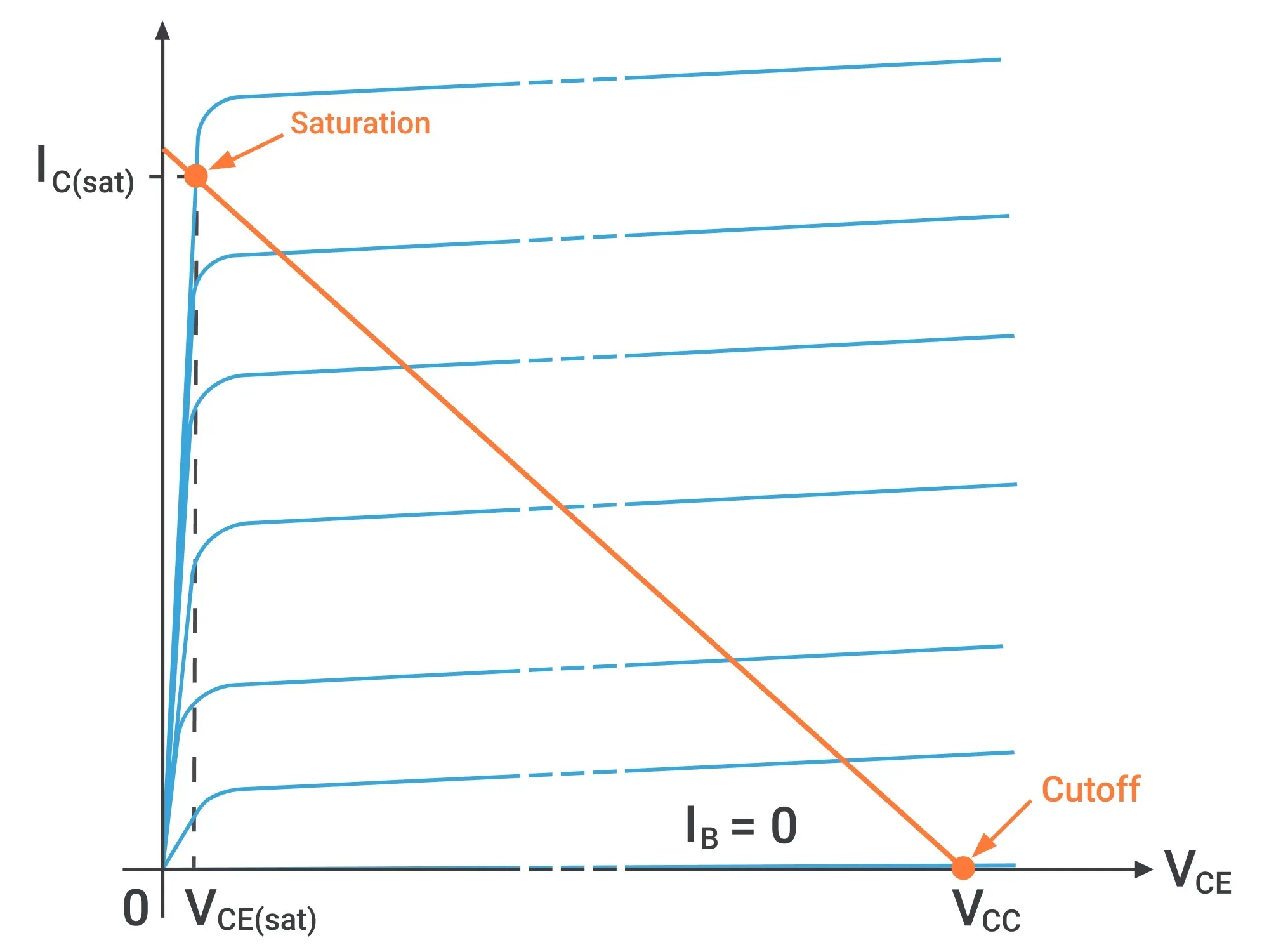
- In the active (amplifying) state, why the collector current Ic is controlled by the base current Ib and appears independent of voltage; that is, why a fixed current gain relationship exists between Ic and Ib. Although the base region is thin, if Ib is zero then Ic is also zero.
- In saturation, why a large reverse collector current Ic can still appear when the collector potential Vc is very low.
Many textbooks do not handle these topics appropriately. Introductory texts often avoid detailed explanations and present conclusions without underlying reasons. Even advanced textbooks sometimes use approaches that create contradictions or confusion. Based on years of teaching and reflection, the following presents an alternative explanation that has been applied in classroom practice. The method is offered for technical discussion and further refinement.
1. Traditional Explanation and Its Problems
The traditional explanation, using an NPN silicon transistor as an example, typically describes three steps: (1) the emitter injects electrons into the base, (2) electrons diffuse and recombine in the base, and (3) the collector collects electrons that have diffused across the base. Several problems arise with this treatment.
Problem 1: In step 3 the formation of collector current Ic is often explained by emphasizing a high Vc and the thin base. This can lead to the incorrect impression that high Vc and a sufficiently thin base are the causes of reverse conduction at the collector junction, and that the PN junction's unidirectional nature fails. This contradicts the current-amplification principle, which requires that in the active state Ic be independent of Vc in magnitude and controlled only by Ib.
Problem 2: The traditional approach fails to explain saturation properly. When the transistor is saturated, Vc can be very low and may even be lower than Vb, yet a large reverse collector current Ic can still occur. This clearly contradicts explanations that rely on a high Vc to produce collector conduction.
Problem 3: Overemphasizing the thin base in step 2 can create the misconception that a sufficiently thin base by itself causes the collector junction to lose PN junction unidirectional behavior. In practice, even with a thin base, the two PN junctions retain their unidirectional characteristics, which is why people can determine transistor terminals by testing junctions.
Problem 4: The traditional explanation does not clearly show why Ic is controlled by Ib and why the current gain remains approximately fixed. Simply citing a thin, lightly doped base from a fabrication perspective does not fundamentally explain the constancy of the current gain.
Problem 5: The standard treatment separates diode and transistor principles rather than building a natural conceptual bridge between them. Diode theory emphasizes PN junction reverse cutoff, while transistor theory is often presented as requiring PN junction reverse conduction. This separation obscures the historical and physical links between diode behavior and transistor amplification.
2. Alternative Explanation
2.1 Starting Point: Diode Behavior
To clarify transistor operation naturally, start from diode principles. A simple PN junction diode has unidirectional conductivity. In reverse bias the PN junction is in cutoff, but a small leakage current still exists. The diode's unidirectional conduction is not absolute.
This leakage arises because, in addition to the majority carriers produced by doping, each region always contains a very small concentration of intrinsic minority carriers. Under reverse bias, the majority carriers are pulled away by the supply so they cannot carry current across the junction, and the residual leakage current is carried mainly by minority carriers. Under reverse bias, minority carriers can cross the junction relatively easily under the influence of the external field; the leakage is small only because the minority carrier concentration is small. Hence the leakage magnitude depends on the number of minority carriers. If one can increase minority carrier concentration under reverse bias, the leakage current will increase. This is the operating principle of a photodiode.
When a photodiode is reverse biased, it exhibits a small dark current (typically on the order of 1e-8 to 1e-9 A). When illuminated, photons generate electron-hole pairs near the junction, dramatically increasing the minority carrier concentration and thus the reverse leakage current. That photocurrent varies with incident light intensity and can be converted to a voltage across a load resistor. The photodiode therefore uses light to control the reverse leakage current of a PN junction.
2.2 Key Conclusion
Emphasize the roles of majority and minority carriers under forward and reverse bias: forward bias conduction is dominated by majority carriers, while reverse bias conduction is dominated by minority carriers. Forward current is large; reverse current is small. Importantly, under reverse bias minority carriers cross the PN junction readily — in fact, the internal field that impedes majority-carrier forward flow assists minority-carrier reverse flow. This is why minority-carrier reverse conduction can be comparatively easy and explains why, in saturation, a transistor's collector junction can still support a substantial reverse current even when Vc is low or near Vb.
2.3 Natural Transition to the Transistor
Continuing from the reverse-biased diode case, if minority-carrier concentration can be increased electrically rather than optically, then reverse leakage can be controlled by electrical injection. To increase the electron minority concentration in a P region electrically, place an N-type region adjacent to the P base as in an NPN transistor structure. This arrangement allows carrier injection into the base region by electrical biasing rather than by light, providing a mechanism to increase the minority-carrier population in the base and thereby control current through the reverse-biased collector junction.


