 ALLPCB


Are you searching for the best HDI PCB design software to create high-density interconnect (HDI) printed circuit boards? Choosing the right tools can make or break your project. In this comprehensive guide, we’ll explore top HDI PCB CAD tools and HDI PCB layout software to help you achieve precision, efficiency, and reliability in your designs. Whether you’re a seasoned engineer or just starting with HDI technology, this blog will walk you through the essentials of selecting software that fits your needs.
At ALLPCB, we understand the importance of having the right tools for complex PCB designs. Let’s dive into the world of HDI PCB design software and uncover the features, benefits, and considerations that will lead you to success.
What is HDI PCB Design and Why Does Software Matter?
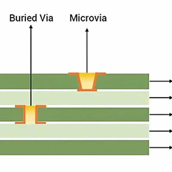
High-Density Interconnect (HDI) PCB design is a specialized approach used to create compact, high-performance circuit boards with a higher wiring density per unit area than traditional PCBs. These boards often feature microvias, blind and buried vias, and fine line widths (sometimes below 3 mils or 0.076 mm). HDI technology is critical for modern electronics, such as smartphones, wearables, and medical devices, where space is limited, and performance is paramount.
The software you choose for HDI PCB design directly impacts your ability to handle these intricate requirements. Unlike standard PCB design, HDI involves tighter tolerances, complex layer stacking (often 8-12 layers or more), and precise signal integrity management (e.g., maintaining impedance values around 50 ohms for high-speed signals). Without the right HDI PCB CAD tools, you risk errors like signal crosstalk, manufacturing delays, or costly redesigns.
Key Features to Look for in HDI PCB Design Software
Not all PCB design tools are equipped to handle the unique challenges of HDI. When selecting the best HDI PCB design software, focus on these critical features to ensure your designs meet industry standards and performance goals.
1. Advanced Layer Management
HDI PCBs often have multiple layers with complex stack-ups. Look for software that supports easy management of 8, 10, or even 12+ layers, allowing you to define via types (through-hole, blind, buried) and control dielectric thickness (e.g., 0.1 mm for high-speed designs). This feature helps maintain signal integrity by minimizing parasitic capacitance.
2. Microvia and Fine Line Support
Microvias, with diameters as small as 0.1 mm, are a hallmark of HDI design. Your software should support the creation and placement of microvias while ensuring compliance with manufacturing constraints. Additionally, it should handle fine line widths and spacing (e.g., 3 mils or less) for dense routing.
3. Signal Integrity Analysis
High-speed signals in HDI PCBs require precise impedance control (often targeting 50-100 ohms) to prevent reflections and crosstalk. Choose software with built-in simulation tools to analyze signal integrity, timing, and electromagnetic interference (EMI) during the design phase.
4. Design Rule Checking (DRC)
HDI designs have strict manufacturing rules due to their complexity. Software with robust DRC capabilities can automatically flag issues like insufficient clearance (e.g., below 0.2 mm) or via stacking errors, saving you from costly revisions.
5. 3D Visualization and Integration
Seeing your HDI PCB in a 3D view helps identify potential issues with component placement or via alignment before manufacturing. Software with 3D visualization and integration with mechanical design tools ensures your board fits perfectly within the final product enclosure.
Top Categories of HDI PCB Layout Software
While specific tools vary, HDI PCB layout software generally falls into categories based on user needs and project complexity. Here’s a breakdown of the types of software you might consider, focusing on their strengths for HDI design.
1. Professional-Grade Tools for Complex HDI Designs
These tools are designed for engineers working on high-end applications like telecommunications or aerospace. They offer advanced features like automated routing for dense layouts, real-time signal integrity analysis, and support for ultra-fine geometries (line widths under 2 mils). While often more expensive, they are indispensable for projects with strict performance requirements, such as maintaining signal speeds above 5 Gbps.
2. Mid-Range Software for Small to Medium Projects
For startups or small teams, mid-range software provides a balance of cost and capability. These tools support HDI designs with up to 8-10 layers and include essential features like microvia placement and basic simulation. They are ideal for consumer electronics where board sizes are small, but budgets are constrained.
3. Free or Open-Source Options for Beginners
If you’re new to HDI PCB design or working on a hobby project, free or open-source software can be a starting point. While they may lack advanced HDI-specific features, some offer basic layer management and routing capabilities. Be cautious, as they might not fully support manufacturing outputs for complex HDI boards, potentially leading to errors in via drilling or spacing.
How to Choose the Best HDI PCB Design Software for Your Needs
Selecting the right HDI PCB CAD tools depends on several factors unique to your project and workflow. Use these steps to narrow down your options and find the perfect fit.
Step 1: Define Your Project Requirements
Start by assessing the complexity of your HDI design. How many layers will your PCB have? Are you working with high-speed signals (e.g., above 1 GHz)? Do you need microvias with aspect ratios of 1:1 or smaller? Understanding these details will help you prioritize software features.
Step 2: Consider Manufacturing Compatibility
HDI PCBs have specific manufacturing requirements, such as laser-drilled vias or sequential lamination. Ensure your software generates output files (like Gerber or ODB++) that align with your manufacturer’s capabilities. At ALLPCB, we provide detailed design guidelines to help you prepare files for seamless production.
Step 3: Evaluate Learning Curve and Support
Some HDI design tools have steep learning curves due to their extensive features. If you’re part of a small team or working solo, opt for software with intuitive interfaces and strong community or technical support. Tutorials and forums can be lifesavers when troubleshooting complex issues like via-in-pad designs.
Step 4: Budget and Licensing
Software costs can range from free to thousands of dollars per license. Determine your budget and whether a subscription or perpetual license works best. Keep in mind that investing in reliable software often saves money by reducing design errors and rework.
Common Challenges in HDI PCB Design and Software Solutions
HDI PCB design comes with unique hurdles. Fortunately, the right software can help overcome these challenges. Here are some common issues and how HDI PCB layout software addresses them.
1. Routing Density
With component densities often exceeding 100 components per square inch, routing in HDI designs is a puzzle. Advanced software offers automated routing algorithms that optimize trace paths while maintaining clearance rules (e.g., 0.15 mm spacing).
2. Thermal Management
Compact HDI boards generate significant heat, especially in power-intensive applications. Software with thermal simulation tools can predict hotspots and suggest via placements or copper pours to dissipate heat effectively.
3. Signal Integrity Issues
High-speed signals are prone to degradation in HDI designs due to short trace lengths and dense layouts. Software with built-in analysis tools can simulate impedance mismatches and recommend adjustments, like adding ground planes or adjusting trace widths to 5 mils for better control.
Tips for Optimizing Your HDI PCB Design Workflow
Beyond choosing the best HDI PCB design software, optimizing your workflow ensures faster turnaround times and higher-quality results. Here are practical tips to enhance your design process.
1. Start with a Clear Schematic
A well-organized schematic is the foundation of any HDI design. Define your net names, power rails, and critical connections early to avoid routing conflicts later.
2. Use Design Libraries
Most HDI software includes libraries of pre-designed components and footprints. Leverage these to save time and ensure accuracy, especially for standard parts like 0402 capacitors or QFN packages.
3. Collaborate with Your Manufacturer
Early collaboration with your PCB manufacturer can prevent design issues. At ALLPCB, we offer design for manufacturability (DFM) checks to ensure your HDI PCB meets production standards, such as minimum via sizes of 0.1 mm or stack-up tolerances.
4. Test Iteratively
Run simulations and DRC checks at multiple stages of your design. Catching errors like insufficient annular rings (e.g., below 0.05 mm) early prevents delays during fabrication.
Why Partner with ALLPCB for Your HDI PCB Projects?
Designing an HDI PCB is only part of the journey. Bringing your design to life requires a reliable manufacturing partner. At ALLPCB, we specialize in producing high-quality HDI PCBs with advanced capabilities like microvias, fine line widths down to 3 mils, and layer counts up to 12 or more. Our team provides expert support from design review to final assembly, ensuring your project meets tight tolerances and performance goals.
With fast turnaround times and competitive pricing, we’re committed to helping engineers and businesses succeed in their HDI PCB endeavors. Trust us to handle the complexities of manufacturing while you focus on creating innovative designs with your chosen HDI PCB CAD tools.
Conclusion: Empower Your HDI PCB Designs with the Right Software
Selecting the best HDI PCB design software is a critical step toward achieving success in your high-density interconnect projects. By focusing on features like advanced layer management, microvia support, and signal integrity analysis, you can tackle the unique challenges of HDI design with confidence. Whether you opt for professional-grade tools or budget-friendly options, ensure the software aligns with your project needs and manufacturing requirements.
At ALLPCB, we’re here to support you every step of the way, from design to delivery. Equip yourself with the right HDI PCB layout software, follow best practices, and partner with us to bring your innovative ideas to life. Start exploring your software options today and take your HDI PCB designs to the next level!


