ALLPCB


Overview
Many embedded-system designs begin with FPGAs to speed prototyping or provide a software development platform. Sometimes FPGAs remain in production designs, but in many cases the plan is to migrate one or more FPGAs to an ASIC for volume manufacturing.
The migration is not automatic. It is not enough to recompile verified FPGA RTL with an ASIC library, validate the generated netlist, and hand files to the backend. The process can be more complex, especially when multiple chips are candidates for integration into a single ASIC or when mixed-signal functionality is required.
Faraday Technology participated in an FPGA-to-ASIC migration for a smart meter. That project illustrates many important subtleties in the migration process and highlights the value of selecting an appropriate design partner.
Smart meter architecture
At first glance a meter seems simple: it monitors the voltage and current on the incoming power lines to a customer premise and records cumulative delivered energy. Traditional meters used electromechanical counters driven by a clever motor.
Smart meters sample voltage and current, digitally accumulate the product, and provide remote readout capability. The design discussed here also includes features such as disconnecting customer power and reporting faults to a network control center when abnormal voltage or current events are detected.
Because most smart meter functionality is implemented in software, the hardware is relatively simple and largely I/O centric (see figure 1). In the customer prototype the hardware included a host processor, an FPGA acting as an I/O hub, various sensors, displays connected mainly via serial interfaces, and a subsystem controller for power-line communication (PLC). The PLC element proved to be an important part of the design.
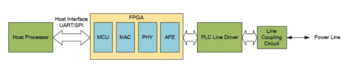
The PLC interface requires a media access controller (MAC), a physical-layer interface (PHY), and an analog front end (AFE). In the prototype all of these functions were implemented in the FPGA, but the PLC interface also required external line drivers and power-line coupling circuits.
The primary goal of the FPGA-to-ASIC migration was cost reduction, partly by eliminating some external components. Meeting demanding ESD and EMI immunity requirements in a challenging environment—especially for an FPGA-based AFE—also placed considerable pressure on the design team.
Migration process
The FPGA-to-ASIC migration involved significant interaction between the design service company and the customer. The outcome was a mixed-signal ASIC based on ARM that reduced the overall chip count (see figure 2).
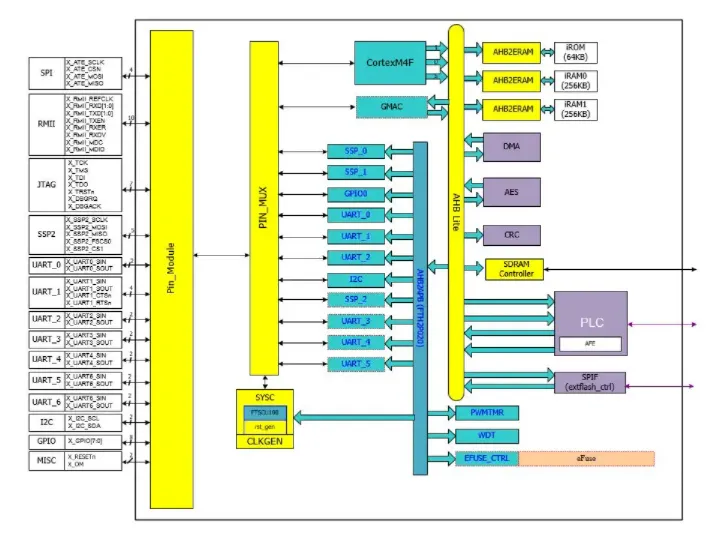
Faraday first evaluated the smart meter architecture. The team concluded that, in addition to replacing the FPGA's existing I/O hub and PLC functions, the ASIC could also assume the host-processor role. This led to a conventional architecture based on an ARM Cortex-M4F core, an AHB-Lite system bus, and an ARM peripheral bus.
The system bus connects interfaces to internal memory and key subsystems, including a MAC, a DMA controller, a CRC controller, and an AES engine for data integrity and security.
Many I/O pins are connected through multiplexing to the peripheral bus. The design includes on-chip ROM and SRAM for the CPU, an e-fuse and controller, and interfaces for external SDRAM and serial flash.
IP consolidation and analog integration
Faraday and the customer selected and configured ASIC IP together. Many FPGA modules were replaced with Faraday, ARM, or third-party ASIC IP blocks. Remaining RTL logic was converted to ASIC, and FPGA phase-locked loops, SRAM instances, and I/O were replaced with equivalent ASIC IP.
The PLC interface was central to the migration, particularly integrating the analog front end into the ASIC. This analog design was challenging because no off-the-shelf IP clearly met the strict ESD and EMI requirements. Faraday's analog design team therefore developed a new AFE.
Faraday performed final SoC and clock-distribution integration and basic functional verification to ensure the parts worked together. The customer performed application-driven validation and software integration. Faraday then completed physical design and signoff verification.
PLC compliance was treated as a special case during verification. The approach to ensuring ESD and EMI compliance was to fabricate a test chip for the AFE and put it through compliance testing on a test bench. Rather than risking a full production run, the team issued a shuttle run for the AFE test chip to enable faster turnaround from the foundry.
Faraday and the customer agreed that the customer would pay for the test chip if it passed compliance tests; if it failed, Faraday would correct the design and provide revised test chips via shuttle. The initial AFE test chip passed, providing significant reassurance to the customer.
Collaboration and outcome
Faraday now supplies the customer with volume SoCs that are assembled and tested.
This smart meter project illustrates that FPGA-to-ASIC migration is not a push-button activity or a one-way contract. When unique functional blocks, special electrical requirements, or chip consolidation opportunities exist, the process requires close collaboration between the customer and the design service company.
Careful evaluation of a design service company's technical capabilities, IP access, experience, and willingness to work closely with the customer team are critical factors that influence the migration outcome, as demonstrated by this smart meter example.