ALLPCB


01. MOSFET breakdown types
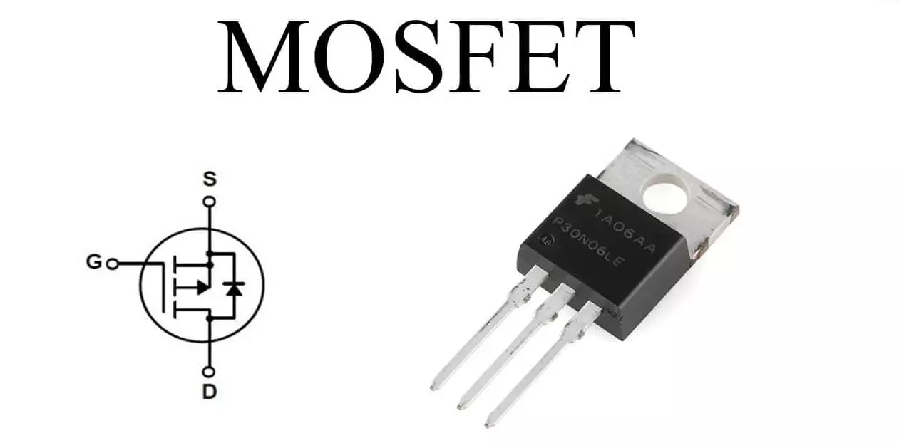
The three terminals of a field-effect transistor are source (S), drain (D) and gate (G). Under common test conditions with source, gate and substrate grounded and the drain voltage swept until the drain current reaches about 1 μA, there are three primary breakdown/leakage paths: drain→source, drain→bulk, and drain→gate.
Drain → Source: punch-through
Punch-through occurs when a reverse bias on the drain expands the drain/bulk depletion region until it reaches the source, creating a conductive path between drain and source without turning on the channel. Preventing punch-through involves process measures such as higher doping at the junctions and punch-through implants or well ties. Layout choices (poly CD, spacer width) and implant profiles (LDD, source/drain implants) also affect susceptibility. If both NMOS and PMOS show the issue, check poly CD and implant steps.
Characteristics of punch-through:
- Soft breakdown point with gradually increasing current as the depletion region expands.
- DIBL and source-bulk forward bias can produce progressively increasing current.
- Not usually destructive, because the peak field is lower than avalanche conditions and does not generate extensive electron-hole pairs.
- Typically occurs in the body of the channel (channel interior) rather than at the surface; it often appears near the channel center.
- Longer poly gate length tends to increase punch-through voltage; effect on avalanche breakdown exists but is less pronounced.
Drain → Bulk: avalanche (PN junction) breakdown
This is classical PN junction avalanche breakdown. Under high reverse bias the depletion region widens and the electric field accelerates carriers that generate additional electron-hole pairs by impact ionization, causing a rapidly increasing current. Avalanche breakdown is typically abrupt and can be destructive if not limited.
Mitigation focuses on reducing peak electric field at the junction by engineering the doping profile (graded junctions, deeper or lighter doping to widen the depletion region). Higher doping concentrations narrow the depletion region and increase the field, reducing breakdown voltage. A simple relation is BV = K*(1/Na + 1/Nb), which shows the lower-doped side dominates the breakdown voltage. If process changes reduce junction BV, investigate source/drain implants and doping profiles.
Drain → Gate: gate oxide or overlap-related breakdown
Overlap between drain and gate can stress the gate oxide and cause gate oxide breakdown, similar to GOX failures. Poly profile and sidewall damage are important factors. Gate-induced drain leakage (GIDL) associated with overlap can also raise leakage and lower apparent breakdown.
In practice, most off-state breakdown cases involve the first two channels. Breakdown can also occur in the on-state if drain voltage is driven excessively high while the gate is biased; this is often seen in NMOS at low gate voltages and is why BVON tests are commonly performed.
02. Overview: MOSFET heating at low currents
MOSFETs are widely used as switches in power and driver circuits. The key conduction parameter is RDS(on), which manufacturers specify as a function of gate-to-source voltage (VGS) and current. With adequate gate drive, RDS(on) is a relatively static parameter. Continuous conduction through a MOSFET causes heating, and rising junction temperature increases RDS(on). Thermal impedance (for example RθJC) defines how effectively the package transfers heat from the semiconductor junction to the case.
03. Causes of MOSFET heating at low currents
- Poor circuit design leaving the MOSFET operating in its linear region rather than fully on. If the MOSFET is not fully enhanced (VGS too low), the voltage drop across it increases, raising dissipation (P = V × I).
- Insufficient gate drive. For N-channel switches, gate voltage must be several volts above source to fully turn on; for P-channel the polarity is reversed.
- High switching frequency. Higher switching frequency increases switching losses and can increase average heating.
- Inadequate thermal design. Even if drain current is below the MOSFET’s peak rating, poor heatsinking or PCB thermal paths can cause high junction temperatures.
- Incorrect device selection. Underestimating on-resistance or switching losses can lead to unexpectedly high dissipation.
04. Practical solutions
- Ensure the MOSFET is fully enhanced in the intended operating condition by providing sufficient gate drive.
- Improve thermal management: add heatsinks, improve PCB copper area, or use thermal vias to carry heat to other layers.
- Use thermal interface materials such as thermal adhesive or pads where appropriate.
- Re-evaluate device selection: choose a MOSFET with lower RDS(on) and adequate SOA for the switching conditions, or split current among parallel devices if needed.
05. MOSFET-based reverse-polarity protection
Series diodes are a simple reverse-polarity protection method, but diode voltage drop can be significant in low-voltage battery systems. Using a MOSFET for reverse-polarity protection yields much lower voltage drop because of its low RDS(on). For example, a MOSFET with 6.5 mΩ RDS(on) at 1 A produces only 6.5 mV drop.
NMOS reverse-polarity protection (low-side or negative rail):
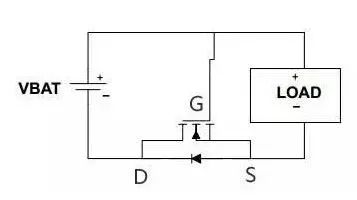
Correct polarity: the MOSFET body diode initially conducts, bringing the source about 0.6 V above ground; the gate sees VBAT so VGS > Vth and the MOSFET turns on, shorting the diode and achieving very low forward drop. Reverse polarity: VGS = 0 so the MOSFET remains off and the load is protected.
PMOS reverse-polarity protection (high-side):
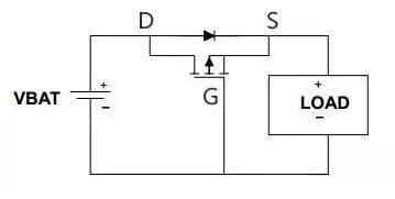
Correct polarity: the body diode conducts at first, the source is VBAT - 0.6 V and the gate at 0 V makes the PMOS conduct, shorting the diode. Reverse polarity: the gate is pulled high and the PMOS stays off, protecting the circuit.
Connection tips: place an NMOS with its D-S path in series with the negative rail, or a PMOS in series with the positive rail, so the intrinsic diode faces the correct current direction during valid connection. MOSFETs allow D and S interchangeability for conduction; this property is used to exploit the body diode during startup so VGS reaches threshold and the FET self-turns on.
06. Measuring MOSFET power loss
Measuring switching losses of MOSFETs and IGBTs is critical during power supply tuning. Switching energy is mainly dissipated during the turn-on and turn-off transitions; conduction losses during the on-state also contribute but the off-state loss is negligible. Accurate measurement requires capturing voltage and current waveforms during switching transitions.
Difference for PFC MOSFETs: unlike ordinary MOSFETs where every switching period looks similar, PFC MOSFETs often have varying voltage and current shapes across cycles. Accurate power-loss assessment for PFC requires longer capture durations (generally > 10 ms), high sampling rate (recommended 1 GS/s), deep memory (recommended > 10 M points) and using all raw samples (no decimation) for the energy calculation.