 ALLPCB


Are you an electronic hobbyist looking to level up your PCB design skills? Understanding PCB impedance design is a key step to ensuring your circuits perform reliably, especially for high-speed or high-frequency projects. If you're searching for "PCB impedance design for beginners," "simple PCB impedance calculation," or "understanding PCB impedance for hobby projects," you're in the right place. In this guide, we'll break down the basics of PCB impedance, explain why it matters, and walk you through simple ways to calculate and design for it in your DIY projects.
This blog post is crafted to be your go-to resource for mastering PCB impedance as a hobbyist. We'll cover the fundamentals, practical design tips, and tools you can use to get started, all explained in an easy-to-follow way. Let's dive into the world of PCB impedance and make your electronic projects more efficient and effective!
What Is PCB Impedance and Why Does It Matter for Hobbyists?
PCB impedance refers to the resistance a circuit board trace offers to alternating current (AC) signals, especially at high frequencies. Think of it as how much a trace "pushes back" against a signal traveling through it. For hobbyists working on simple projects like LED circuits or basic microcontrollers, impedance might not be a big concern. But as soon as you step into high-speed designs—such as USB interfaces, RF circuits, or fast digital signals—it becomes critical.
Why does it matter? If the impedance isn't controlled, signals can reflect back along the trace, causing interference, data loss, or even circuit failure. For example, in a USB 2.0 design, the differential impedance should be around 90 ohms to ensure proper signal transmission at speeds up to 480 Mbps. Mismatched impedance can lead to errors or dropped connections. By understanding and designing for impedance, you ensure signal integrity, reduce noise, and make your projects more reliable.

Key Concepts in PCB Impedance for Beginners
Before we get into calculations and design tips, let’s cover some basic concepts related to PCB impedance. These will help you grasp the bigger picture and apply the knowledge to your hobby projects.
1. Types of Impedance in PCB Design
There are two main types of impedance to consider:
- Single-Ended Impedance: This applies to a single trace carrying a signal, common in simpler designs. It’s the impedance between the trace and the ground plane.
- Differential Impedance: This is used for pairs of traces, like in USB or Ethernet designs, where two traces carry complementary signals. It’s the impedance between the two traces.
For most beginner projects, single-ended impedance is what you’ll deal with, but understanding differential impedance is useful as you advance to complex designs.
2. Factors Affecting Impedance
Impedance isn’t just a random number—it depends on several physical aspects of your PCB:
- Trace Width: Wider traces have lower impedance because they can carry more current with less resistance.
- Trace Thickness: Thicker traces (measured in ounces of copper, like 1 oz or 2 oz) also lower impedance.
- Dielectric Material: The PCB substrate (like FR-4) affects impedance through its dielectric constant, typically around 4.2 to 4.5 for standard materials.
- Trace Length: Longer traces can introduce more impedance and signal delay.
- Distance to Ground Plane: The closer a trace is to the ground plane, the lower the impedance due to increased capacitance.
By tweaking these factors, you can control impedance to match your design needs.
Why Hobbyists Should Care About Impedance in DIY Projects
As a hobbyist, you might wonder if impedance design is overkill for small-scale projects. While it’s true that low-speed circuits (like a simple Arduino setup running at 16 MHz) may not require strict impedance control, many modern DIY projects do. Here are a few examples:
- High-Speed Digital Circuits: If you're working with microcontrollers or FPGA boards communicating at speeds above 50 MHz, impedance mismatches can distort signals.
- RF Projects: Radio frequency designs, such as Wi-Fi modules or amateur radio circuits, often require a specific impedance (like 50 ohms) for antennas and transmission lines.
- Sensor Interfaces: Some sensors output high-frequency signals that can degrade without proper impedance matching.
By learning impedance design now, you’ll be prepared for more advanced projects and avoid troubleshooting headaches later.
Simple PCB Impedance Calculation for Beginners
Calculating PCB impedance might sound intimidating, but it’s manageable with the right approach. While precise calculations often require professional software, hobbyists can use simplified methods and online tools to get close enough for most DIY projects. Let’s walk through the process step by step.
Step 1: Understand Your Target Impedance
First, determine the impedance value your design needs. Common values include:
- 50 ohms for RF circuits and coaxial cable connections.
- 90 ohms for differential pairs in USB 2.0.
- 100 ohms for differential pairs in Ethernet designs.
Check the datasheet of the components or protocol you're using to find the required impedance.
Step 2: Gather PCB Parameters
Next, collect data about your PCB design:
- Trace width (e.g., 10 mils or 0.254 mm).
- Trace thickness (e.g., 1 oz copper, which is about 1.4 mils or 0.035 mm thick).
- Dielectric thickness (distance between trace and ground plane, often 4-8 mils for standard boards).
- Dielectric constant of the material (around 4.2 for FR-4).
These values depend on your board’s stack-up, which you can usually get from your PCB manufacturer or design software.
Step 3: Use a Simplified Formula or Tool
For single-ended microstrip traces (a common setup where the trace is on the top layer above a ground plane), a simplified formula for impedance (Z0) is:
Z0 = (87 / √(Er + 1.41)) * ln(5.98 * H / (0.8 * W + T))
Where:
- Z0 = Characteristic impedance in ohms.
- Er = Dielectric constant (e.g., 4.2 for FR-4).
- H = Dielectric thickness (height between trace and ground plane, in mils).
- W = Trace width (in mils).
- T = Trace thickness (in mils).
For example, let’s calculate the impedance of a trace with W = 10 mils, T = 1.4 mils, H = 6 mils, and Er = 4.2:
- First, √(4.2 + 1.41) = √5.61 ≈ 2.37
- 87 / 2.37 ≈ 36.7
- Inside the ln: (5.98 * 6) / (0.8 * 10 + 1.4) = 35.88 / 9.4 ≈ 3.82
- ln(3.82) ≈ 1.34
- Z0 ≈ 36.7 * 1.34 ≈ 49.2 ohms
This trace would have an impedance of roughly 50 ohms, which is ideal for many RF applications.
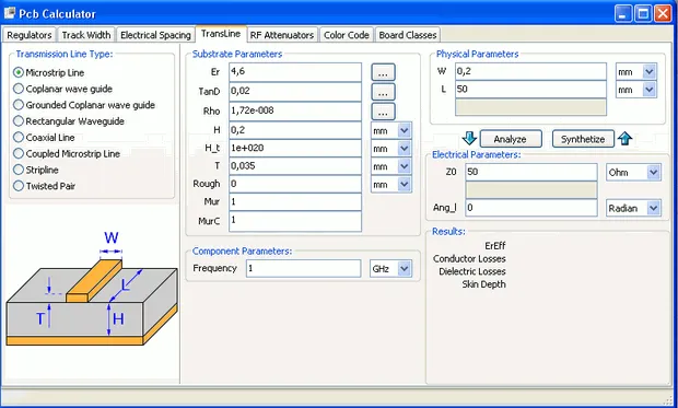
If math isn’t your thing, don’t worry. Many free online calculators can do this for you. Simply input your trace dimensions and material properties to get an approximate impedance value.
Step 4: Adjust Trace Width for Desired Impedance
If the calculated impedance doesn’t match your target, adjust the trace width. A wider trace lowers impedance, while a narrower trace increases it. Recalculate or use a tool to find the right width. For hobbyists, getting within 10% of the target impedance is often good enough for non-critical designs.
Practical Tips for PCB Impedance Design in Hobby Projects
Now that you understand the basics of calculating impedance, let’s look at some actionable tips to apply in your DIY PCB designs.
1. Stick to Standard Stack-Ups
For most hobby projects, use a standard two-layer or four-layer PCB with a ground plane directly below signal traces. This setup, called a microstrip configuration, makes impedance control easier. A typical two-layer board with 1.6 mm thickness and 1 oz copper works well for beginners.
2. Keep Traces Short and Direct
Long traces can introduce unwanted impedance and signal delays. Route high-speed signals as straight and short as possible to minimize these effects.
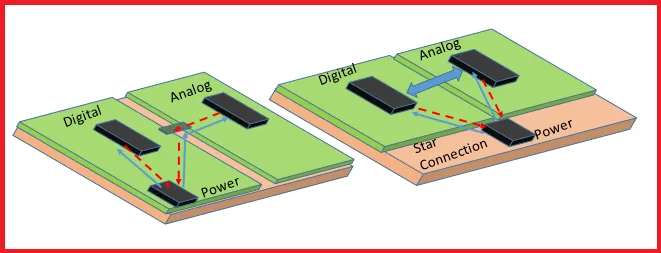
3. Use Ground Planes
A solid ground plane beneath your signal traces helps maintain consistent impedance and reduces noise. Avoid splitting the ground plane under high-speed traces, as this can disrupt impedance.
4. Test and Iterate
As a hobbyist, you might not have access to expensive testing equipment. However, you can still prototype your design, test it with an oscilloscope if possible, and look for signal distortions. If something’s off, adjust trace widths or layouts and try again.
Tools and Resources for PCB Impedance Design
You don’t need to do everything manually. Here are some tools and resources to simplify impedance design for hobbyists:
- Free Online Calculators: Many websites offer free impedance calculators where you input trace dimensions and get instant results.
- PCB Design Software: Most design tools have built-in impedance calculators or wizards to help you set trace widths based on target impedance.
- Manufacturer Guidelines: When ordering your PCB, check with the fabrication house for stack-up details and impedance control options. Many provide free resources or support for hobbyists.
Common Mistakes to Avoid in PCB Impedance Design
As a beginner, it’s easy to make mistakes when dealing with impedance. Here are a few pitfalls to watch out for:
- Ignoring Stack-Up: Not considering the distance to the ground plane or dielectric material can lead to incorrect impedance values.
- Inconsistent Trace Widths: Changing trace widths along a signal path disrupts impedance. Keep them uniform.
- Neglecting High-Speed Signals: Even if your project seems simple, check if any signals operate at high frequencies that require impedance control.
Conclusion: Start Designing with Impedance in Mind
Mastering PCB impedance design might seem like a daunting task for electronic hobbyists, but it’s a valuable skill that can take your projects to the next level. By understanding the basics of PCB impedance, using simple calculation methods, and following practical design tips, you can ensure better signal integrity and performance in your DIY circuits. Whether you're working on a high-speed digital project or an RF module, impedance control is within your reach with the right tools and knowledge.
Start small by experimenting with trace widths and using free online calculators to get a feel for how impedance works. As you gain confidence, you’ll find that designing for impedance becomes second nature. Keep learning, prototyping, and refining your skills, and soon you’ll be creating professional-quality PCBs for all your hobby projects.


