ALLPCB


Product overview
In electronic design, high-precision, low-noise analog-to-digital converters (ADC) are a frequent requirement for engineers. This article examines the high-performance, four-channel, 20-bit current-input ADC from Texas Instruments, the DDC114.
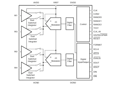
The DDC114 is a highly integrated single-chip solution designed for direct measurement of four low-level currents. It integrates current-to-voltage conversion and A/D conversion, allowing direct connection of four low-level current-output devices, such as photodiodes, and digitizing their outputs. This design simplifies circuit implementation and improves overall system performance.
Key features
- High accuracy: true integration architecture with integral linearity up to ±0.01% of reading plus 0.5 ppm of full-scale range (FSR), providing very precise measurements.
- Low noise: noise as low as 5.2 ppm of FSR (rms), ensuring high sensitivity and accuracy for low-level signal measurements.
- Low power: typical power per channel is 13.5 mW, suitable for power-sensitive applications.
- Adjustable data rate: data rate selectable up to 3.125 kSPS.
- Programmable full-scale range: full-scale range adjustable from 12 pC to 350 pC to suit different application needs.
- Cascadable serial interface: supports cascading multiple devices for larger measurement systems.
Applications
The DDC114 is suitable for applications such as CT scanner data acquisition systems (DAS), photodiode sensors, infrared pyrometers, and liquid/gas chromatography instruments.
Electrical characteristics
Analog input range
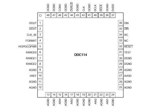
The DDC114 provides eight selectable analog input ranges from 12 pC to 350 pC. The range is selected via the RANGE0–RANGE2 pins, allowing adaptation to different current signal amplitudes.
Dynamic characteristics
- Data rate: up to 2.5 kSPS in low-power mode; up to 3.125 kSPS in high-speed mode.
- Integration time: TINT adjustable from 50 us to 1 s, enabling a trade-off between measurement precision and throughput.
- System clock input: the system clock (CLK) frequency can be adjusted according to operating mode and application requirements.
Accuracy specifications
- Noise: 5.2 ppm of FSR (rms) for low-level inputs (<1% FSR), supporting high-precision measurements of weak signals.
- Integral linearity error: typical ±0.01% of reading + 0.5 ppm of FSR; maximum ±0.025% of reading + 1.0 ppm of FSR.
- Resolution: selectable via the FORMAT pin. FORMAT = 1 selects 20-bit output; FORMAT = 0 selects 16-bit output.
Operational principle
Basic architecture
Internally, the DDC114 contains four identical input channels. Each channel includes two integrators that perform continuous current-to-voltage integration. Integrator outputs are routed through two 4-input multiplexers to two delta-sigma (ΣΔ) converters for A/D conversion.
Integration cycle
The front-end analog integrator consists of an operational amplifier, a selectable feedback capacitor network (CF), and multiple switches. Controlling these switches implements integrate, reset, hold, and convert states. During a conversion cycle, the integration capacitor is first reset to the reference voltage (VREF), then integrates the input signal, and finally the integrator result is digitized.
Voltage reference
The external voltage reference (VREF) is critical for DDC114 operation. It is used to reset the integrator before the integration interval and as the reference during conversion. To ensure VREF stability and low noise, buffering the external reference with an operational amplifier is recommended.
Digital interface and operating modes
Digital interface
The DDC114 provides digital results via a synchronous serial interface, including differential data clocks (DCLK and DCLK), a data valid signal (DVALID), differential serial data outputs (DOUT and DOUT), and differential serial data inputs (DIN and DIN). This interface simplifies cascading multiple devices and data transfer.
Operating modes
- Low-power mode: HISPD/LOPWR = 0 selects low-power operation. Typical power per channel is 13.5 mW, with a maximum data rate of 2.5 kSPS.
- High-speed mode: HISPD/LOPWR = 1 selects high-speed operation. Typical power per channel is 18.0 mW, with a maximum data rate of 3.125 kSPS.
Data retrieval
In continuous and non-continuous modes, data can be retrieved after DVALID goes low. Data is shifted out on the falling edge of DCLK. To avoid introducing noise, stop data retrieval while the CONV signal is changing.
Layout and power considerations
Power supply
AVDD and DVDD supplies should be kept as quiet as possible to minimize noise impact on measurements. Two supply options are common: using two isolated +5 V supplies for AVDD and DVDD with 10 uF solid tantalum and 0.1 uF ceramic decoupling capacitors; or deriving DVDD from AVDD through an isolation resistor of less than 10 ohm.
Grounding
Connect analog ground (AGND) and digital ground (DGND) to the same ground plane on the PCB to reduce ground noise.
Shielding
Due to the DDC114's high input impedance and sensitivity to external noise, apply shielding measures in PCB layout. Placing a grounded PCB plane around input pins helps reduce coupling noise and leakage currents.
Summary
The DDC114 combines high accuracy, low noise, low power, and flexible configuration, making it suitable for many high-precision current measurement applications. In practice, select operating mode, integration time, and input range according to application requirements, and pay careful attention to power supply design, grounding, and shielding to realize the device's performance.