 ALLPCB


Are you a hobbyist eager to level up your electronics projects by creating a multi-layer PCB at home? With the sequential build-up method, DIY multi-layer PCB fabrication is within your reach. This guide walks you through the entire process, from understanding the basics to mastering PCB etching techniques, PCB lamination for hobbyists, and even creating vias at home. Let’s dive into the step-by-step journey of building a professional-quality multi-layer PCB in your own workspace.
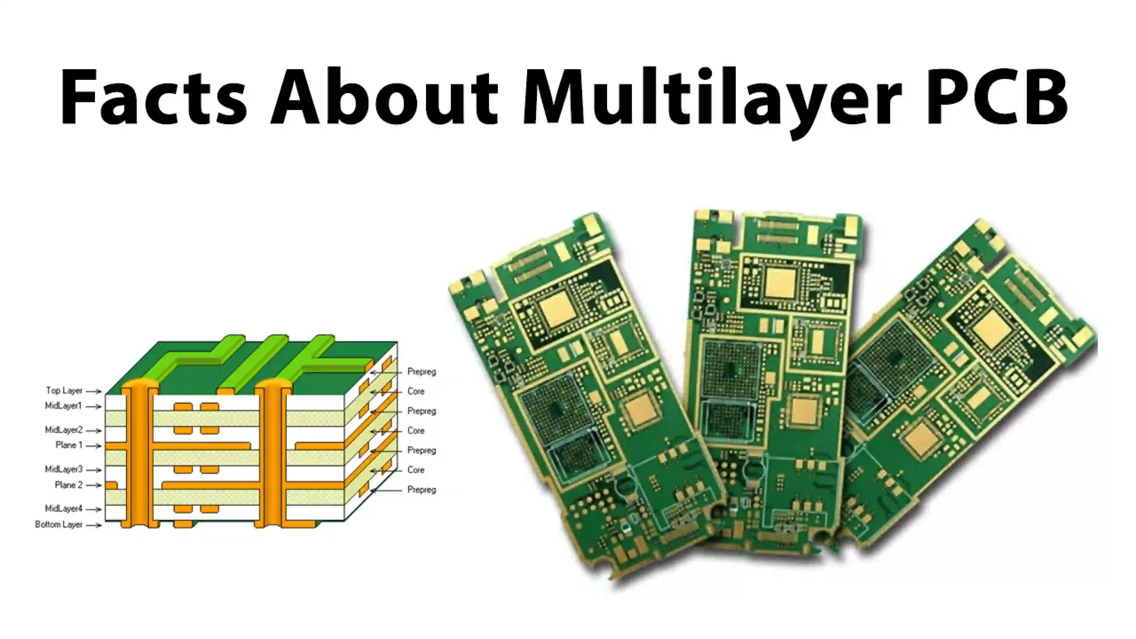
What Is a Multi-Layer PCB and Why Build One at Home?
A multi-layer PCB (Printed Circuit Board) consists of more than two layers of conductive copper, separated by insulating material, all stacked together to form a single board. These boards are essential for complex electronics, as they allow for denser circuits, better signal integrity, and reduced electromagnetic interference. For hobbyists, creating a multi-layer PCB at home offers cost savings, rapid prototyping, and the freedom to customize designs for unique projects.
Building a multi-layer PCB using the sequential build-up method means adding layers one at a time, aligning and bonding them carefully to ensure functionality. While this process can be challenging, it’s achievable with the right tools, patience, and techniques. This blog will break down every step to help you succeed.
Benefits of DIY Multi-Layer PCBs for Hobbyists
Before we get into the how-to, let’s explore why you might want to take on this project:
- Cost-Effective: Professional multi-layer PCB fabrication can be expensive, especially for small runs. DIY saves money.
- Customization: Tailor your board to specific needs without relying on standard manufacturing constraints.
- Learning Experience: Mastering PCB etching techniques and lamination at home builds valuable skills for future projects.
- Quick Prototyping: No need to wait weeks for a manufacturer; test your designs in days.
Tools and Materials Needed for DIY Multi-Layer PCB Fabrication
To start your journey in sequential build-up at home, gather these essential tools and materials. Having everything ready will streamline the process and reduce errors.
- Copper-Clad Boards: Thin, double-sided boards for each layer (e.g., 0.8mm or 1.6mm thickness).
- Prepreg Sheets: Insulating material for bonding layers (fiberglass epoxy sheets).
- Etching Solution: Ferric chloride or sodium persulfate for PCB etching techniques.
- Toner Transfer Paper or Photoresist Film: For transferring your circuit design to the copper.
- Laminator or Iron: For toner transfer or PCB lamination for hobbyists.
- Drill Bits and Drill Press: For creating vias at home (0.3mm to 1mm bits).
- Conductive Ink or Rivets: To connect vias between layers.
- Heat Press or Oven: For bonding layers during sequential build-up.
- Protective Gear: Gloves, goggles, and a well-ventilated workspace for safety during etching.
- Design Software: Use free tools to create and print your PCB layouts.
Ensure you have a clean, organized workspace to avoid contamination or misalignment during the build.
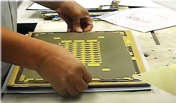
Step-by-Step Guide to Creating a Multi-Layer PCB at Home
Now, let’s walk through the detailed process of building a multi-layer PCB using sequential build-up at home. Follow these steps carefully for the best results.
Step 1: Design Your Multi-Layer PCB Layout
Start by designing each layer of your PCB using software. Plan the placement of components, traces, and vias to ensure proper alignment across layers. For a 4-layer board, you’ll typically have:
- Top layer: Signal or component layer.
- Inner layer 1: Ground plane.
- Inner layer 2: Power plane.
- Bottom layer: Signal or additional components.
Export each layer as a separate high-resolution image or PDF for printing. Ensure vias (holes connecting layers) are marked clearly, as they’re critical for functionality.
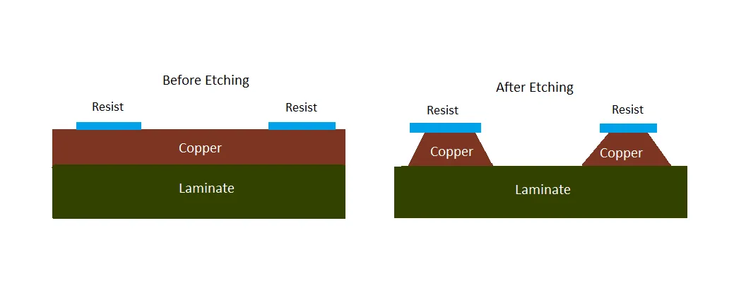
Step 2: Prepare and Etch Individual Layers Using PCB Etching Techniques
With your designs ready, it’s time to transfer them onto copper-clad boards using PCB etching techniques. Here’s how:
- Print the Design: Use a laser printer to print each layer’s design onto toner transfer paper or photoresist film. Ensure the print is mirrored for correct orientation.
- Transfer the Design: Place the printed design face-down on a cleaned copper-clad board. Use a laminator or iron to transfer the toner by applying heat and pressure for 2-3 minutes.
- Etch the Board: Submerge the board in an etching solution like ferric chloride (diluted to 1:3 ratio with water) for 10-20 minutes. Agitate gently to speed up the process. The copper not covered by toner will dissolve, leaving your traces. Rinse with water and remove the toner with acetone.
Repeat this for each layer of your multi-layer PCB. Double-check alignment marks to ensure layers will stack correctly.
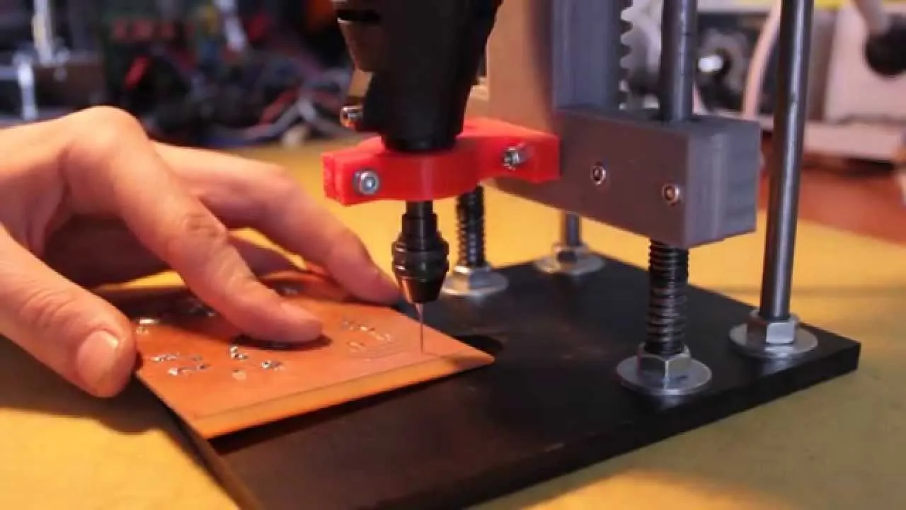
Step 3: Drill Vias for Inter-Layer Connections
Creating vias at home is a crucial step for connecting layers. Vias are small holes drilled through the board, later filled or plated to conduct electricity between layers.
- Mark Via Locations: Use your design as a guide to mark via positions on each layer.
- Drill Holes: Use a drill press with a small bit (0.3mm to 0.8mm) for precision. Drill through all layers after temporary alignment to ensure holes match up.
- Connect Vias: For a simple DIY method, insert small copper rivets or use conductive ink to fill the holes. This creates a conductive path between layers. For better reliability, consider electroplating if you have access to the setup (though this requires more advanced tools).
Ensure vias are clean and free of debris before moving to lamination.
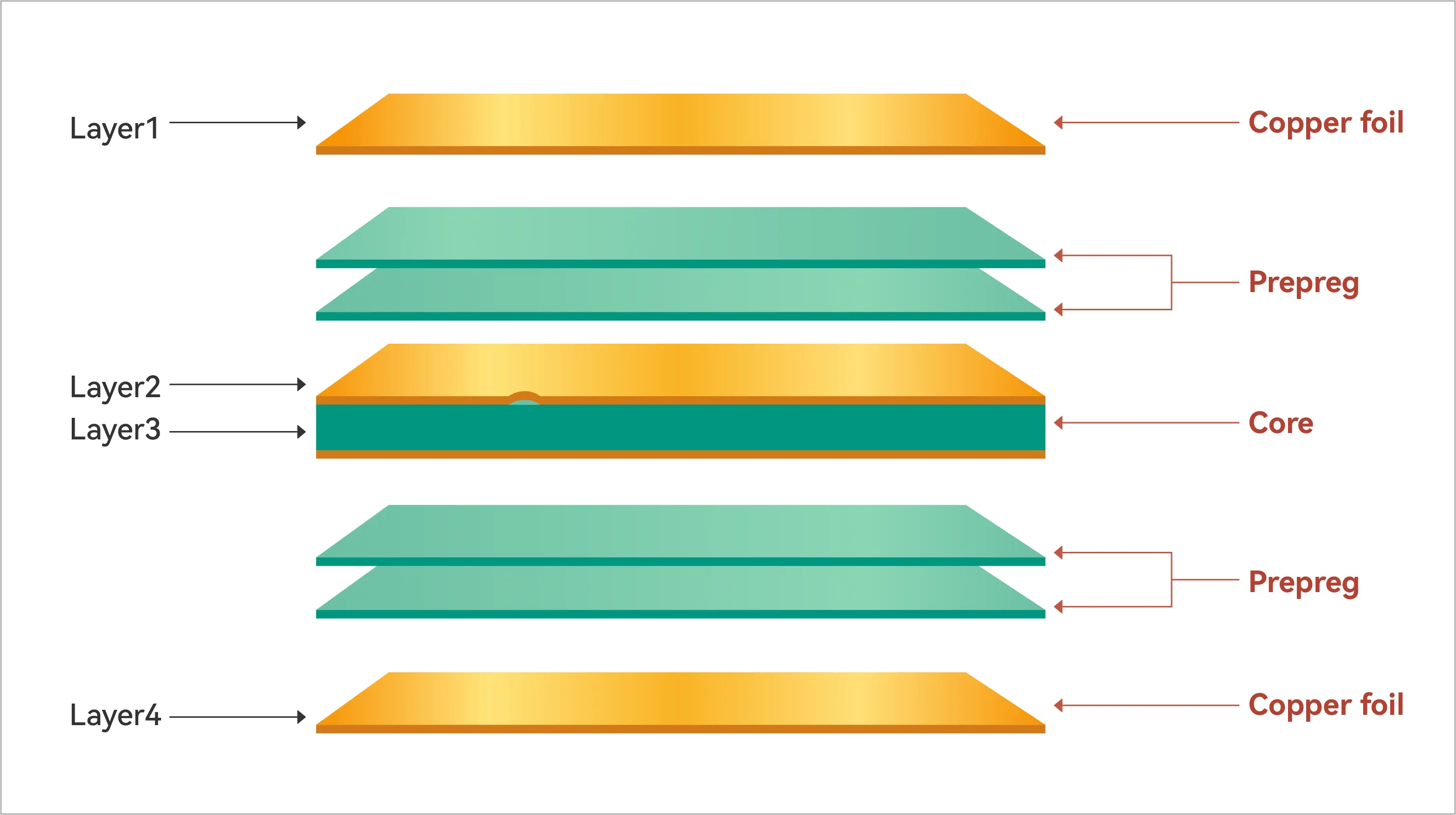
Step 4: Laminate Layers with Sequential Build-Up at Home
PCB lamination for hobbyists involves bonding the etched layers together with insulating material (prepreg) using heat and pressure. Sequential build-up means adding one layer at a time, ensuring alignment and bonding before moving to the next.
- Prepare Layers: Stack your etched boards with prepreg sheets between them. Prepreg is a partially cured epoxy-fiberglass material that hardens under heat. Use 1-2 sheets (about 0.1mm thick each) per layer gap for insulation.
- Align Layers: Use alignment pins or marks to ensure traces and vias line up perfectly. Misalignment can ruin connectivity.
- Bond with Heat and Pressure: Place the stack in a heat press or DIY setup (e.g., between metal plates in an oven) at 170-180°C for 1-2 hours with even pressure (around 50-100 psi if measurable). This cures the prepreg, bonding the layers into a solid board.
- Cool Slowly: Let the board cool under pressure to avoid warping.
After lamination, inspect the board for bubbles or delamination, which indicate poor bonding. Repeat the process for each additional layer if building more than two at a time.
Step 5: Finalize and Test Your Multi-Layer PCB
Once all layers are laminated, finalize your board:
- Trim Excess Material: Cut the board to its final size using a saw or rotary tool.
- Clean and Inspect: Remove any residue and check for continuity between vias and traces using a multimeter.
- Add Components: Solder components onto the board, ensuring connections work as designed.
- Test Functionality: Power up your circuit and verify signal integrity. Multi-layer PCBs often handle high-speed signals (e.g., up to 100 MHz or more), so test for noise or interference. If impedance control is critical, aim for consistent trace widths (e.g., 0.2mm for 50-ohm lines) during design.
If issues arise, trace them back to specific layers or vias and troubleshoot accordingly.
Challenges and Tips for Successful DIY Multi-Layer PCB Fabrication
Building a multi-layer PCB at home comes with challenges. Here are common issues and tips to overcome them:
- Misalignment: Use alignment holes or pins before etching and lamination. Double-check designs for accuracy.
- Poor Via Connections: Test vias with a multimeter after drilling and filling. Redrill or refill if conductivity fails.
- Delamination: Ensure even heat and pressure during lamination. Avoid rushing the cooling process.
- Etching Errors: Use fresh etching solution and monitor the process closely to avoid over-etching traces.
Patience is key. Start with a simple 3-layer board before attempting more complex designs with 6 or more layers.
Safety Precautions for PCB Etching and Lamination at Home
Working with chemicals and heat requires caution. Follow these safety tips:
- Always wear gloves and goggles when handling etching solutions like ferric chloride, as they can irritate skin and eyes.
- Work in a well-ventilated area to avoid inhaling fumes during etching or lamination.
- Store chemicals in labeled, sealed containers away from children or pets.
- Use heat-resistant gloves when handling hot presses or ovens during lamination.
Why Sequential Build-Up Is Ideal for Hobbyists
The sequential build-up method is particularly suited for hobbyists because it allows control over each layer’s addition. Unlike pressing all layers at once (which requires industrial equipment), sequential build-up lets you verify alignment and connections step by step. This reduces errors and makes the process manageable with basic tools.
Conclusion: Start Your DIY Multi-Layer PCB Journey Today
Creating a multi-layer PCB at home with sequential build-up is a rewarding challenge for any electronics hobbyist. By mastering PCB etching techniques, PCB lamination for hobbyists, and creating vias at home, you can produce complex, professional-quality boards without breaking the bank. Follow the steps outlined in this guide, stay patient, and experiment with small projects to build your skills.
Whether you’re designing a high-speed circuit or a compact device, the ability to craft a DIY multi-layer PCB opens up endless possibilities. Gather your tools, plan your design, and start building today. With practice, you’ll be amazed at what you can achieve in your home workshop.


