ALLPCB


In the world of electronics, producing high-quality printed circuit boards (PCBs) at a reasonable cost is a top priority for engineers and manufacturers. One powerful technique to achieve both quality and affordability is strategic controlled depth drilling, often referred to as back drilling. But how does controlled depth drilling help reduce PCB costs while optimizing performance? Simply put, it removes unnecessary via stubs in multi-layer PCBs, improving signal integrity for high-speed designs and reducing manufacturing defects—ultimately saving time and money.
In this comprehensive guide, we’ll dive deep into how controlled depth drilling works, why it’s a game-changer for PCB optimization, and how it fits into cost-effective manufacturing and design for manufacturing (DFM) strategies. Whether you’re an engineer looking to enhance signal performance or a manufacturer aiming to streamline production, this blog will provide actionable insights to help you succeed.
What is Controlled Depth Drilling and Back Drilling?
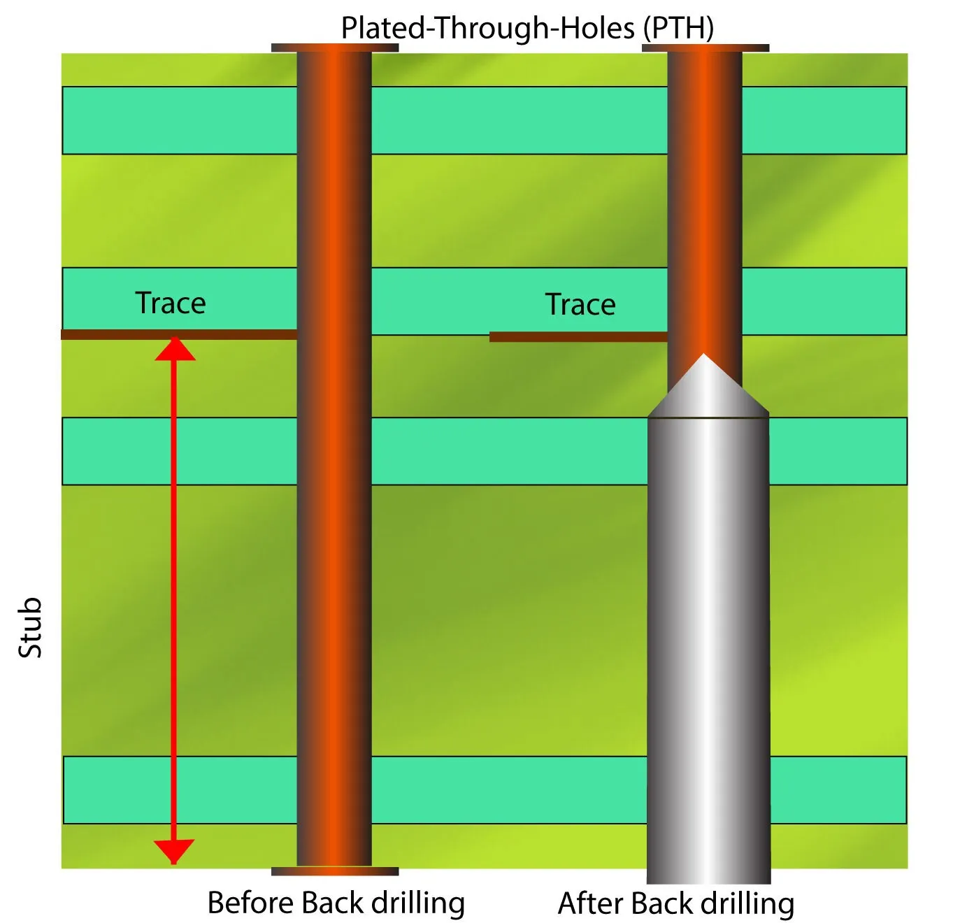
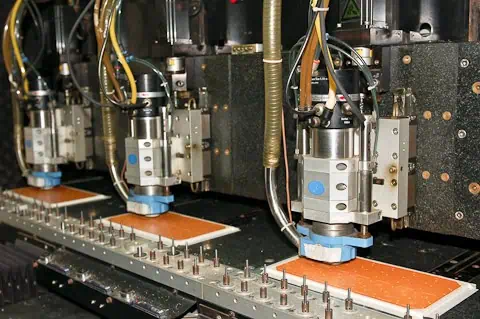
Controlled depth drilling, commonly known as back drilling, is a specialized manufacturing process used in multi-layer PCB production. It involves drilling into a plated through-hole (PTH) via from the opposite side of the board to remove the unused portion of the copper barrel, also called a via stub. These stubs, if left in place, can cause signal reflections and distortions, especially in high-speed designs operating at frequencies above 1 GHz.
By precisely controlling the depth of the drill, manufacturers can eliminate these stubs without damaging the functional parts of the via. This process not only boosts signal integrity but also reduces the risk of manufacturing errors, making it a cost-effective solution for complex PCB designs. Back drilling is particularly valuable in applications like telecommunications, data centers, and high-speed computing, where signal quality is critical.
Why Controlled Depth Drilling Matters for PCB Optimization
PCB optimization is all about balancing performance, reliability, and cost. Controlled depth drilling plays a crucial role in this balance by addressing one of the biggest challenges in high-speed designs: signal integrity. Let’s break down why this technique is so important.
1. Improved Signal Integrity
In high-speed PCBs, via stubs act like tiny antennas, causing signal reflections that degrade performance. For example, in a design operating at 10 Gbps, a via stub as short as 0.5 mm can introduce enough reflection to cause data errors. Back drilling removes these stubs, ensuring cleaner signal transmission and reducing the need for costly redesigns or additional components like equalizers.
2. Reduced Electromagnetic Interference (EMI)
Via stubs can also contribute to EMI, which interferes with nearby components and circuits. By eliminating these stubs through controlled depth drilling, you minimize EMI, leading to a more reliable design without the need for extra shielding or filtering—both of which add to PCB costs.
3. Enhanced Design Flexibility
Back drilling allows engineers to use thicker boards with more layers without worrying about stub-related issues. This flexibility is essential for complex designs where space and layer count are critical, enabling optimized layouts without sacrificing performance.
How Controlled Depth Drilling Supports Cost-Effective PCB Manufacturing
While controlled depth drilling might seem like an added step in the manufacturing process, it actually contributes to significant cost savings in the long run. Here’s how it aligns with cost-effective PCB manufacturing goals.
1. Minimizes Redesign and Testing Costs
Signal integrity issues caused by via stubs often lead to failed prototypes and multiple redesign cycles. Each redesign can cost thousands of dollars in engineering time and materials. By implementing back drilling early in the design process, you reduce the likelihood of these issues, saving both time and money.
2. Reduces Component Costs
Without back drilling, engineers might need to add components like termination resistors or advanced signal conditioning circuits to compensate for signal distortions. These components not only increase the bill of materials (BOM) cost but also add complexity to the design. Controlled depth drilling eliminates the need for such workarounds, keeping costs down.
3. Lowers Manufacturing Defect Rates
Back drilling requires precision, but modern manufacturing equipment can achieve tolerances as tight as ±0.05 mm. This precision reduces the risk of over-drilling or damaging functional vias, leading to fewer defective boards and less waste during production. Fewer defects mean lower overall manufacturing costs.
Integrating Controlled Depth Drilling into Design for Manufacturing (DFM)
Design for Manufacturing (DFM) is a critical approach to PCB development that focuses on creating designs that are easy and cost-effective to produce. Controlled depth drilling fits perfectly into DFM principles by addressing potential manufacturing challenges early in the design phase. Here are key ways to integrate back drilling into your DFM strategy.
1. Plan Via Placement Early
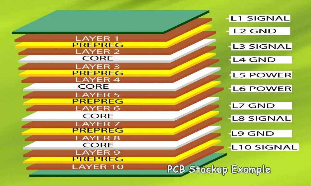
During the PCB layout stage, identify which vias will require back drilling based on signal paths and layer transitions. For instance, vias connecting inner layers in a 10-layer board are prime candidates for back drilling if they don’t need to extend to outer layers. Planning ahead ensures that drilling depths and tolerances are accounted for in the design files.
2. Communicate with Your Manufacturer
Collaboration between designers and manufacturers is essential for successful back drilling. Provide detailed documentation, including drill depth specifications and target impedance values (e.g., 50 ohms for single-ended signals). Clear communication prevents misunderstandings and ensures the drilling process aligns with your design goals.
3. Optimize Layer Stackup
A well-thought-out layer stackup can minimize the need for extensive back drilling. For example, placing high-speed signal layers closer to the top or bottom of the board reduces via stub length, making back drilling more effective and less costly. Tools like simulation software can help model impedance and signal behavior before finalizing the stackup.
Best Practices for Implementing Controlled Depth Drilling
To maximize the benefits of controlled depth drilling while keeping PCB costs low, follow these best practices during design and manufacturing.
1. Use Simulation Tools for Signal Analysis
Before finalizing your design, use simulation tools to analyze signal integrity and identify vias with problematic stubs. These tools can predict how a stub of 0.3 mm might affect a signal at 5 GHz, allowing you to prioritize back drilling where it’s most needed.
2. Specify Tolerances Clearly
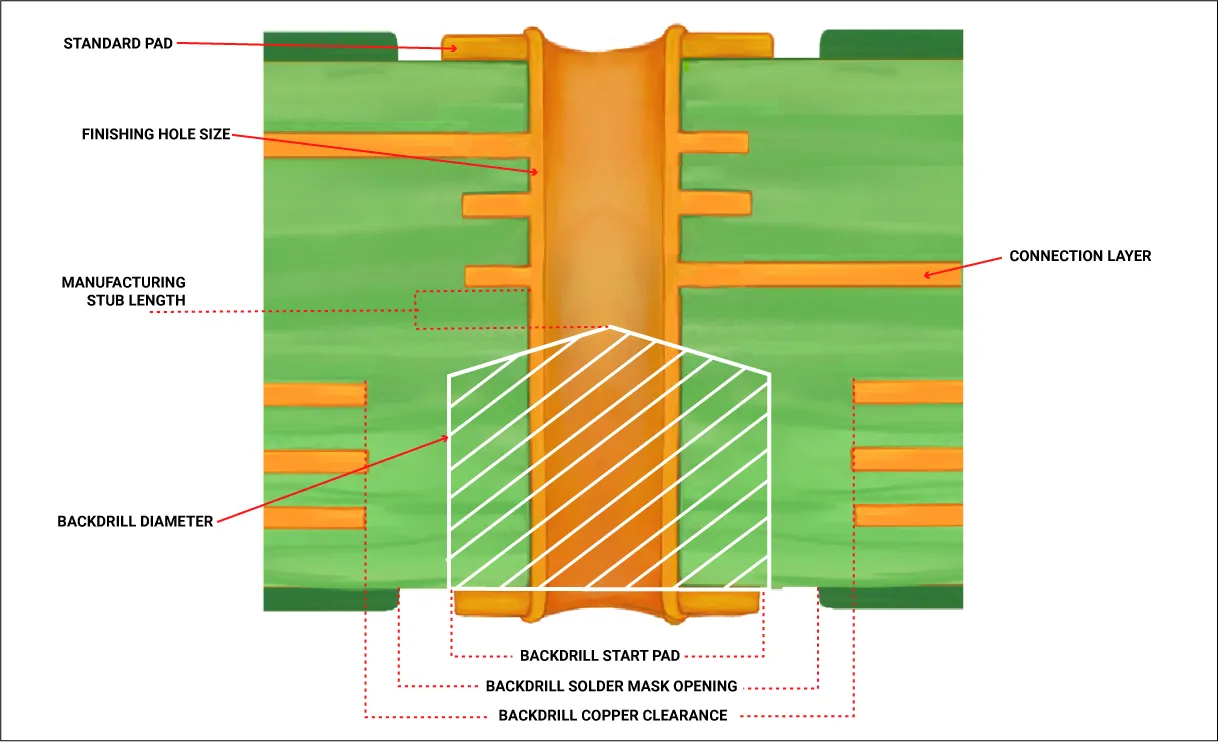
When defining back drilling parameters, specify tight tolerances for drill depth and diameter. A typical back drill diameter might be 0.2 mm larger than the original via to ensure complete stub removal without affecting the functional barrel. Clear specifications prevent manufacturing errors and costly rework.
3. Test Prototypes Thoroughly
After manufacturing, test your prototypes to verify signal performance and confirm that back drilling achieved the desired results. Use tools like time-domain reflectometry (TDR) to measure impedance and detect any remaining reflections. Testing ensures that your design is ready for mass production without hidden issues.
Challenges and Solutions in Controlled Depth Drilling
While controlled depth drilling offers many advantages, it’s not without challenges. Understanding these hurdles and how to overcome them is key to successful implementation.
Challenge 1: Precision Drilling Requirements
Back drilling demands high precision to avoid damaging functional parts of the via. Modern drilling machines can achieve depth accuracy within ±0.025 mm, but even small errors can lead to signal issues.
Solution: Partner with a manufacturer equipped with advanced drilling technology and strict quality control processes. Ensure that your design files include precise drill depth data to guide the process.
Challenge 2: Increased Manufacturing Time
Adding a back drilling step can extend production timelines, especially for complex boards with hundreds of vias.
Solution: Optimize your design to minimize the number of vias requiring back drilling. Focus on critical high-speed signals and use alternative routing strategies where possible to reduce drilling needs.
Challenge 3: Higher Initial Costs
The upfront cost of back drilling can be a concern for small-batch production or budget-conscious projects.
Solution: Weigh the initial cost against long-term savings from fewer redesigns and improved reliability. For high-volume production, the per-unit cost of back drilling decreases significantly, making it a worthwhile investment.
The Future of Controlled Depth Drilling in PCB Manufacturing
As electronics continue to push the boundaries of speed and complexity, controlled depth drilling will become even more critical. Emerging technologies like 5G, artificial intelligence, and the Internet of Things (IoT) demand PCBs that can handle frequencies above 25 GHz with minimal signal loss. Back drilling will play a central role in meeting these demands while keeping manufacturing costs manageable.
Additionally, advancements in drilling technology, such as laser-based depth control, are making the process faster and more precise. These innovations will further reduce PCB costs and open new possibilities for design optimization, ensuring that manufacturers and engineers can stay ahead in a competitive market.
Conclusion: Balancing Cost and Performance with Controlled Depth Drilling
Controlled depth drilling, or back drilling, is a proven technique for achieving cost-effective PCB manufacturing without compromising on performance. By removing via stubs, it enhances signal integrity, reduces EMI, and minimizes the need for costly redesigns and additional components. When integrated into a solid design for manufacturing strategy, it helps engineers and manufacturers create high-quality boards that meet the demands of modern electronics.
From planning via placement to collaborating with manufacturers and testing prototypes, every step of implementing back drilling contributes to PCB optimization. While challenges like precision and initial costs exist, the long-term benefits far outweigh the drawbacks, especially for high-speed applications.
By adopting controlled depth drilling as part of your PCB design and manufacturing process, you’re not just cutting costs—you’re building a foundation for reliable, high-performing electronics. Start exploring this technique today to stay competitive in an ever-evolving industry.