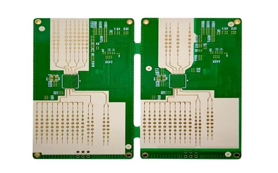
In the world of PCB manufacturing, reducing costs without sacrificing quality is a top priority for engineers and designers. One of the most effective ways to achieve this is by mastering the use of breakaway tabs in PCB panelization. But what exactly are breakaway tabs, and how do they contribute to PCB manufacturing cost reduction? In this comprehensive guide, we’ll explore how breakaway tabs work, compare breakaway tabs vs routing cost, dive into PCB panelization cost analysis, and share tips for optimizing breakaway tab design for cost and low-cost PCB assembly. Let’s uncover the strategies that can save you money and streamline your production process.
What Are Breakaway Tabs and Why Do They Matter?
Breakaway tabs, often referred to as "mouse bites," are small, perforated connections used to hold individual printed circuit boards (PCBs) together within a larger panel during manufacturing. These tabs are designed to be strong enough to keep the boards secure during assembly but weak enough to be easily broken apart after production. This technique is a cornerstone of PCB panelization, a process that groups multiple boards on a single panel to maximize efficiency.
The primary reason breakaway tabs matter is their impact on cost. By allowing multiple PCBs to be manufactured and assembled as a single unit, they reduce material waste, minimize handling time, and lower overall production expenses. For engineers looking to achieve low-cost PCB assembly, understanding and utilizing breakaway tabs can make a significant difference in both small-scale and mass production.
The Role of PCB Panelization in Cost Reduction
Before diving deeper into breakaway tabs, let’s understand the broader concept of PCB panelization and its role in PCB manufacturing cost reduction. Panelization involves arranging multiple individual PCBs onto a single larger board for manufacturing. This approach offers several benefits:
- Material Efficiency: Producing multiple boards on one panel reduces wasted substrate material, lowering raw material costs by as much as 20-30% in some cases.
- Faster Assembly: Automated assembly machines can process an entire panel at once, cutting down on setup and handling time.
- Reduced Labor Costs: Handling fewer panels means less manual intervention, which translates to lower labor expenses.
However, the method used to separate individual boards from the panel—whether through breakaway tabs, routing, or other techniques—plays a critical role in determining the overall cost and efficiency. This is where a detailed PCB panelization cost analysis becomes essential.
Breakaway Tabs vs Routing Cost: Which Is More Cost-Effective?
When it comes to separating individual PCBs from a panel, two common methods stand out: breakaway tabs and tab routing. Let’s break down the breakaway tabs vs routing cost comparison to help you decide which is better for your project.
Breakaway Tabs: Pros and Cons
Breakaway tabs use small, perforated sections to connect PCBs within a panel. These perforations are typically created using a series of small holes (mouse bites) that make it easy to snap the boards apart manually or with minimal tools.
- Advantages:
- Lower Cost: Breakaway tabs are generally cheaper to implement than routing because they don’t require additional milling or cutting processes. This can save up to 10-15% on depaneling costs for high-volume production.
- Simpler Process: No specialized equipment is needed for separation, reducing setup expenses.
- Less Material Waste: Since no material is removed (as in routing), there’s minimal waste, contributing to overall PCB manufacturing cost reduction.
- Disadvantages:
- Rough Edges: Breaking boards apart can leave small burrs or rough edges, which may require additional finishing for high-precision applications.
- Limited to Simple Shapes: Breakaway tabs work best for rectangular or simple board shapes, as complex outlines can complicate tab placement.
Tab Routing: Pros and Cons
Tab routing, on the other hand, involves using a CNC machine to mill narrow tabs that hold the PCBs together. After assembly, the boards are separated by cutting or breaking these tabs.
- Advantages:
- Cleaner Edges: Routing provides smoother edges compared to breakaway tabs, which is ideal for boards requiring precise dimensions or aesthetic finishes.
- Flexible Design: Suitable for complex board shapes and irregular outlines, offering greater design freedom.
- Disadvantages:
- Higher Cost: Routing requires specialized machinery and additional processing time, increasing costs by 15-25% compared to breakaway tabs in many scenarios.
- More Waste: Material is removed during milling, leading to higher waste and impacting overall cost efficiency.
Cost Verdict: For most projects focused on low-cost PCB assembly, breakaway tabs are the more economical choice due to their simplicity and reduced processing requirements. However, if your design demands precision edges or complex shapes, the added expense of routing may be justified.
PCB Panelization Cost Analysis: How Breakaway Tabs Save Money
Conducting a thorough PCB panelization cost analysis is key to maximizing savings in manufacturing. Breakaway tabs contribute to cost reduction in several ways, which we’ll explore with some estimated figures based on industry standards.
- Reduced Depaneling Costs: Depaneling with breakaway tabs often requires no additional machinery, saving approximately $0.05 to $0.10 per board compared to routing or other methods in high-volume runs (based on typical production of 1,000+ units).
- Lower Material Costs: Since breakaway tabs don’t remove material during separation, you can fit more boards on a panel without worrying about spacing for milling paths. This can increase panel yield by 5-10%, directly impacting material efficiency.
- Faster Production Time: Manual or simple tool-based separation with breakaway tabs cuts down on production bottlenecks, potentially reducing assembly time by 10-20% compared to machine-based routing processes.
However, it’s important to balance these savings with potential trade-offs, such as the need for post-separation finishing if rough edges are a concern. By carefully designing tab placement and size, you can minimize these issues and further enhance cost-effectiveness.
Optimizing Breakaway Tab Design for Cost
While breakaway tabs are inherently cost-effective, optimizing breakaway tab design for cost can amplify their benefits. Here are practical design tips to ensure you’re getting the most value out of this technique:
1. Strategic Tab Placement
Place tabs in areas that minimize stress on critical components during separation. Avoid placing tabs near sensitive parts or connectors, as snapping the board can cause micro-cracks or damage. Typically, placing 2-3 tabs per side for small boards (under 4 inches) and 4-5 tabs for larger ones ensures stability without overcomplicating separation.
2. Use Standard Tab Sizes
Stick to industry-standard tab sizes, such as 0.2-0.3 inches wide with 5-7 small holes (mouse bites) for perforation. Custom sizes may increase manufacturing complexity and cost, whereas standard configurations are easier and cheaper to produce.
3. Minimize Tab Count
While you need enough tabs to hold the board securely during assembly, using too many increases the effort required for separation and can lead to more rough edges. Aim for the minimum number of tabs necessary to maintain structural integrity during production—often determined by board size and weight.
4. Consider Board Shape and Size
For non-rectangular boards, position tabs at points where stress is evenly distributed during breaking. If your design allows, opt for simpler shapes to make tab implementation more straightforward and cost-effective.
Best Practices for Low-Cost PCB Assembly with Breakaway Tabs
Achieving low-cost PCB assembly goes beyond just using breakaway tabs. It requires a holistic approach to design and manufacturing. Here are some best practices to integrate breakaway tabs into your workflow for maximum savings:
- Collaborate Early with Manufacturers: Share your panelization design with your manufacturing partner during the planning stage. They can provide insights on tab placement and panel layout to avoid costly revisions. Early collaboration can reduce production errors by up to 15%.
- Test Separation Before Full Production: Create a prototype panel to test how easily the boards separate and whether any components are at risk. This step can prevent expensive rework in large-scale runs.
- Balance Panel Size: While larger panels increase yield, they can also increase handling difficulty and risk of damage. Aim for a panel size that fits within standard manufacturing equipment limits (often 18x24 inches) to avoid custom processing fees.
- Document Specifications: Clearly specify tab dimensions, hole spacing (e.g., 0.04-inch diameter holes spaced 0.08 inches apart), and placement in your design files to avoid miscommunication with the manufacturer.
Common Challenges with Breakaway Tabs and How to Overcome Them
While breakaway tabs are a powerful tool for cost savings, they come with challenges. Here’s how to address common issues:
- Rough Edges After Separation: If aesthetics or precision are critical, consider light sanding or specify a secondary finishing process. This adds minimal cost (around $0.02 per board) compared to routing.
- Component Damage Risk: Ensure components are placed at least 0.1 inches away from tab areas to avoid stress during breaking. Use simulation tools to predict stress points if needed.
- Tab Breakage During Assembly: If tabs break prematurely, increase tab width or reduce the number of perforations. Testing different configurations on a small batch can help find the right balance.
Conclusion: Unlocking Cost Savings with Breakaway Tabs
In the quest for PCB manufacturing cost reduction, breakaway tabs stand out as a simple yet highly effective solution. By understanding the nuances of breakaway tabs vs routing cost, conducting a detailed PCB panelization cost analysis, and focusing on optimizing breakaway tab design for cost, you can significantly lower expenses while maintaining quality. These strategies, combined with best practices for low-cost PCB assembly, empower engineers and designers to streamline production and maximize efficiency.
Implementing breakaway tabs isn’t just about cutting costs—it’s about smart design and planning. With the right approach, you can transform your PCB manufacturing process into a model of cost-effectiveness and precision. Start incorporating these techniques into your next project and experience the benefits firsthand.
 ALLPCB


