ALLPCB


A discussion in a user group prompted a brief summary of common diode uses in LDO circuits.
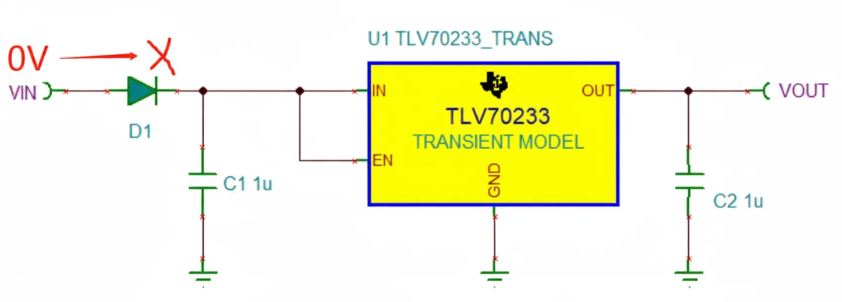
1. Reverse-connection protection — diode in series with VIN
Place a diode in series with the VIN input, as shown for D1 below. This serves two purposes: it prevents the power supply from being connected in reverse, and in applications with a large VIN-to-VOUT drop the diode can absorb part of the thermal dissipation of the LDO.
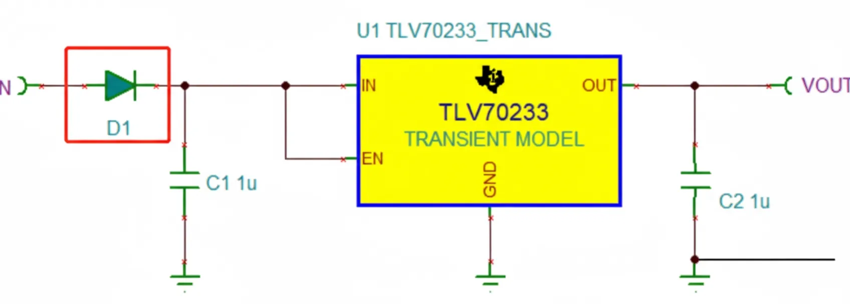
Principle
If VIN and GND are reversed, the series diode D1 prevents ground from reaching the LDO, so no current loop forms and the LDO is protected.
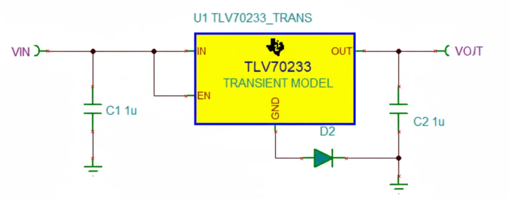
2. Reverse-connection protection — diode between system GND and LDO ground
A diode can also be placed between the system ground and the LDO chip ground, as shown for D2. When VIN and GND are reversed, D2 prevents VIN from reaching the LDO, so no current loop forms and the LDO is protected.
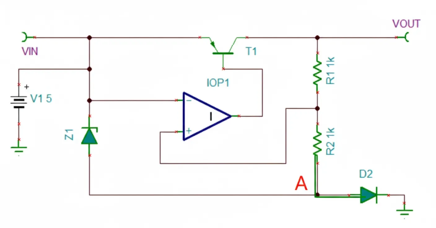
Because of D2, the LDO ground (node A) is elevated by roughly the forward voltage drop of D2.
For older PNP-based LDO architectures, raising node A will reduce VOUT. Replacing the diode with a voltage source and plotting the DC transfer characteristic shows that as V2 (node A) increases, VOUT decreases.
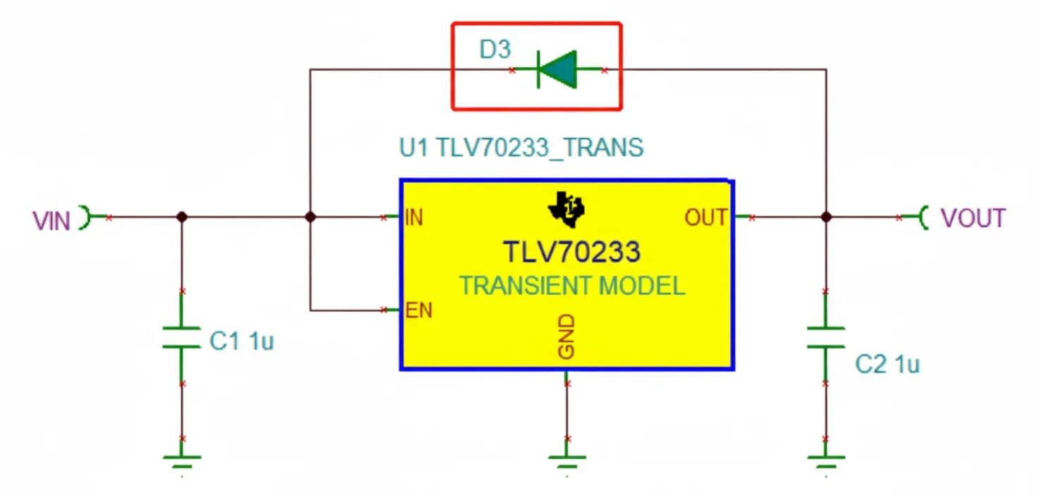
3. Input-output clamping protection
Place a diode between the input and output to prevent reverse voltages from damaging the LDO. Typical behavior:
- When the LDO is operating normally, VIN is higher than VOUT and diode D3 is reverse-biased.
- During power-down, if VOUT falls more slowly than VIN, a reverse differential can occur and damage the LDO. Diode D3 clamps the input-output differential to approximately the diode forward drop, protecting the LDO.
This is common for older LDO architectures using PNP transistors, since the emitter-collector reverse voltage tolerance can be limited.
4. Voltage drop and backfeed prevention
In less-demanding scenarios, place a diode D4 in series with the output to add a small voltage drop to reach the desired output level and to prevent VOUT from backfeeding into the chip OUT pin.