ALLPCB


1. Filter Basics
1.1 Filter definition
GB/T 2900.1-2008 Electrotechnical terms: basic terms defines a filter as a two-port linear device designed according to specified rules to pass certain spectral components of an input quantity while attenuating others. In general, a filter is a network of lumped resistors, capacitors, and inductors, or distributed inductance and capacitance, that allows some frequencies to pass and suppresses others. In practice, a filter is a frequency-selective circuit.
1.2 Filter classification
1.2.1 Classification by frequency characteristics (amplitude and phase response)
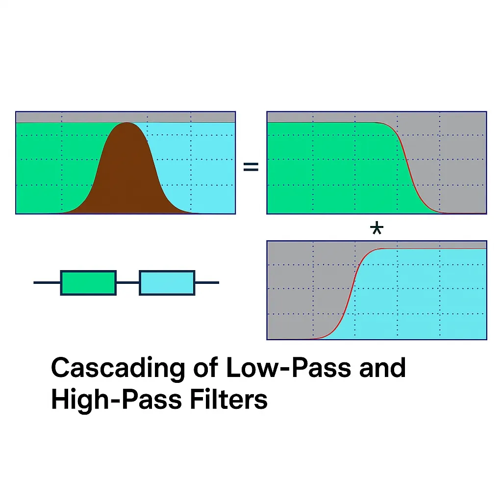
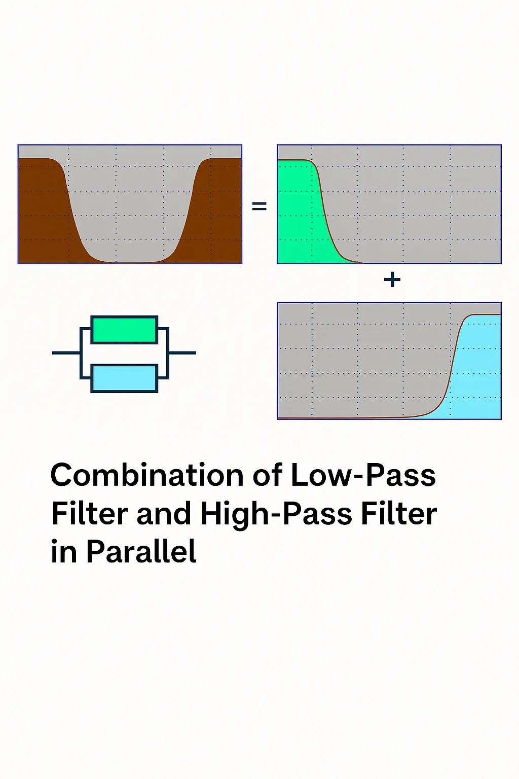
Filters can be divided into low-pass, high-pass, band-pass, and band-stop types.
Low-pass filter
Between 0 and f2 the amplitude response is flat, allowing frequency components below f2 to pass without attenuation while strongly attenuating components above f2.
High-pass filter
The opposite of a low-pass filter. From f1 to infinity the amplitude response is flat, allowing frequency components above f1 to pass with little attenuation while strongly attenuating components below f1.
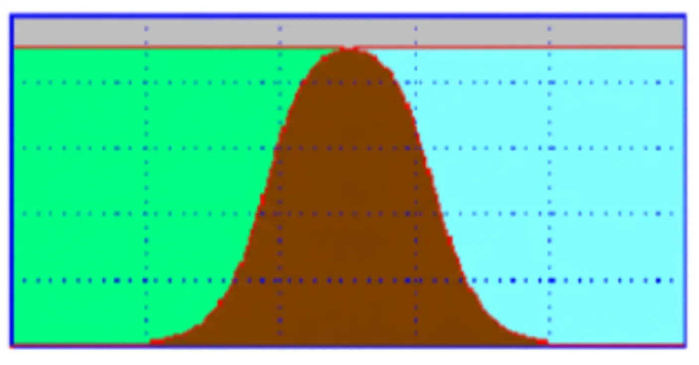
Band-pass filter
Within the passband f1 to f2 it allows components above f1 and below f2 to pass without attenuation, while attenuating other components.
Band-stop filter
Opposite of a band-pass filter. The stopband is between f1 and f2, attenuating components in that range while allowing other frequencies to pass with little attenuation.
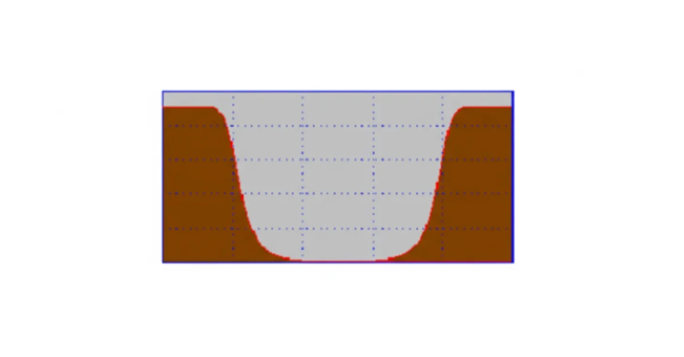
Band-stop filter frequency response
Low-pass and high-pass are the two basic forms; other filters can be decomposed into these types. A series connection of low-pass and high-pass forms a band-pass, while a parallel connection forms a band-stop.
1.2.2 Classification by energy loss characteristics
Filters can be reflective (lossless) or absorptive (lossy).
Reflective filters
Reflective filters, also called lossless filters, operate by creating a large impedance discontinuity in the signal path so that most electromagnetic energy is reflected back toward the source. Reflective filters use passive energy-storage elements such as inductors L and capacitors C, and provide good frequency selectivity, but they are prone to resonance.
Absorptive filters
Absorptive filters use lossy components so that the energy of interfering signals is dissipated within the filter. They avoid resonances caused by parasitics or impedance mismatch, but have poorer frequency selectivity. Absorptive filters typically use ferrite or other lossy materials, with wires passed through or wound on ferrite shapes to use inductance and eddy-current losses to block interference propagation.
1.2.3 Classification by approximation criteria
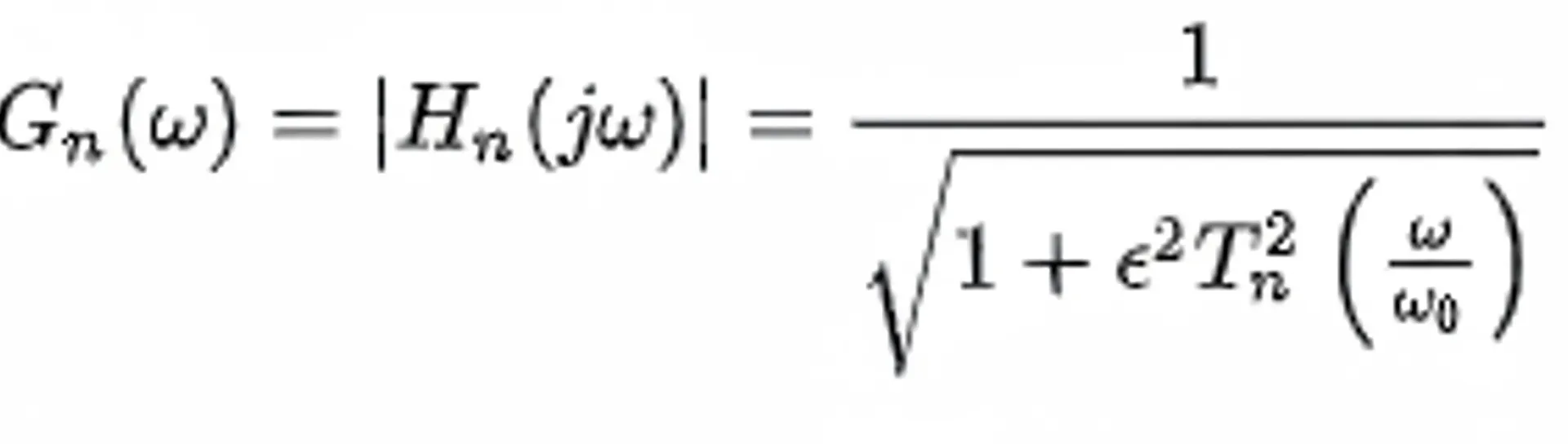
Filters include Butterworth, Chebyshev, and Bessel types.
Butterworth filter
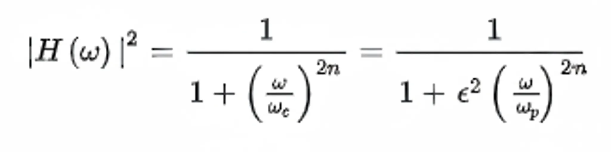
Defined by amplitude response requirements without considering phase. The Butterworth filter provides maximally flat amplitude in the passband, with no ripple, and gradually rolls off toward zero in the stopband.
The squared amplitude of an nth-order Butterworth low-pass filter can be expressed by the following formula:
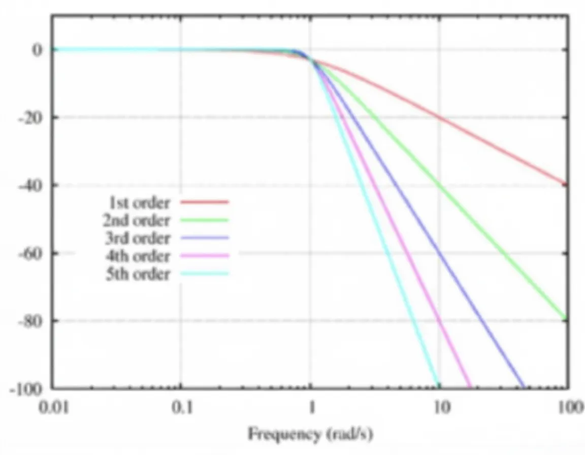
Butterworth low-pass responses for orders 1 through 5
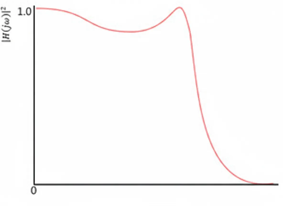
Chebyshev filter
The Chebyshev filter exhibits equiripple behavior in the passband or stopband. It is named after the Russian mathematician Pafnuty Chebyshev.
Compared with a Butterworth filter, a Chebyshev filter rolls off faster in the transition band but has less flatness in the passband. The Chebyshev response minimizes the error between the filter and an ideal response, at the cost of passband ripple.
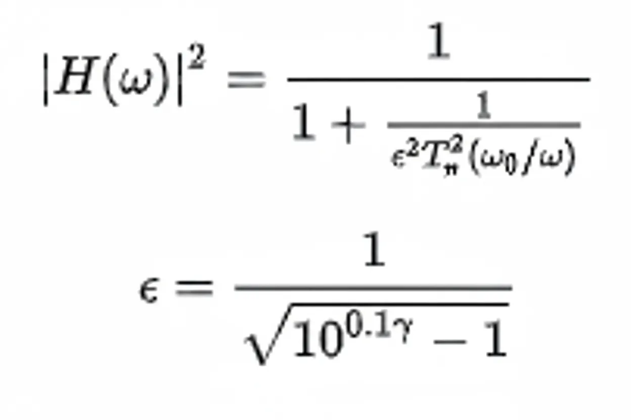
Type I Chebyshev filter: the amplitude-to-frequency relationship can be expressed as follows:
Type I Chebyshev response curves
Type II Chebyshev filter
Also called the inverse Chebyshev filter. It is less common because its cutoff roll-off is not as rapid as Type I and it does not require more components. Type II has no passband ripple but exhibits ripple in the stopband.
The transfer function of a Type II Chebyshev filter is:
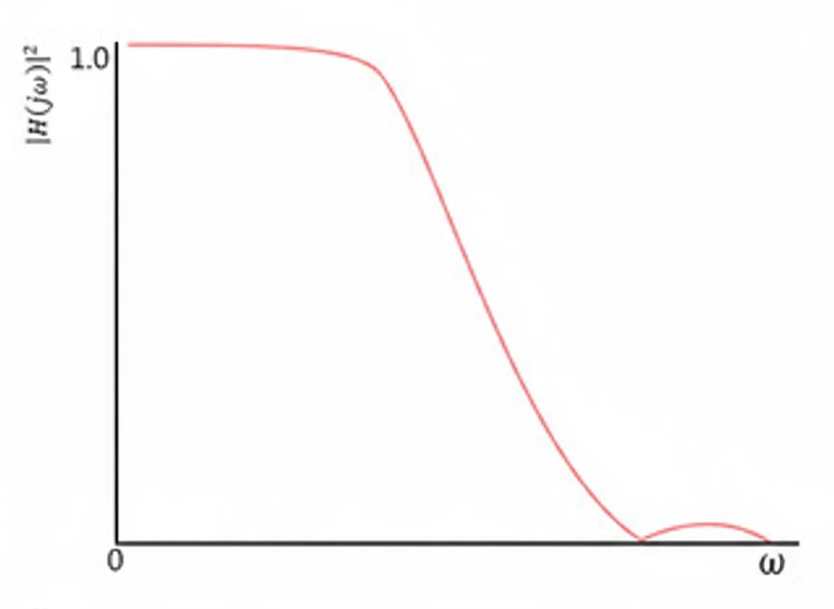
Type II Chebyshev response curves
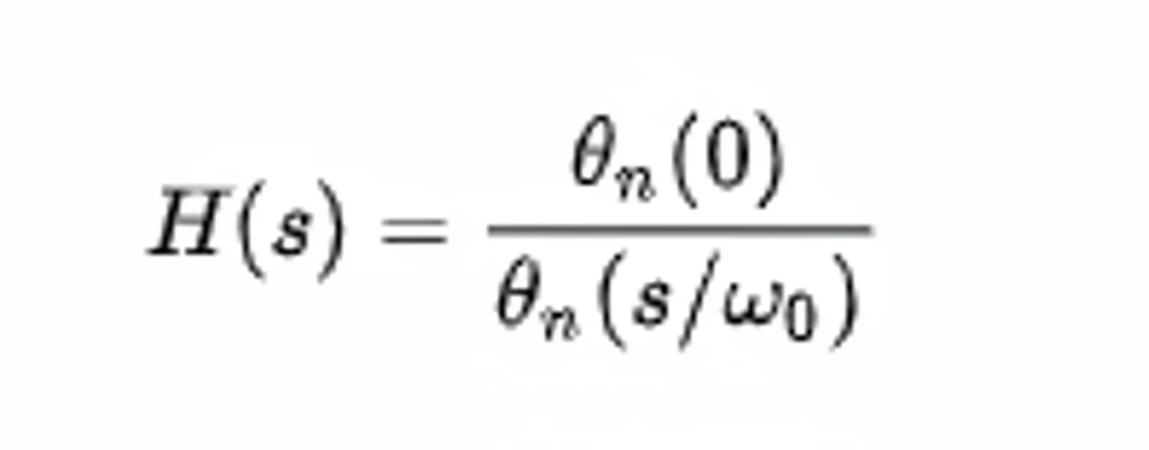
Bessel filter
The Bessel filter has the flattest group delay and nearly linear phase in the passband. Because it provides nearly constant delay for frequencies below the cutoff, it is used in audio equipment where preserving phase relationships is important while attenuating out-of-band noise. The transfer function for a Bessel low-pass filter is:
2. Nonidealities of Filters
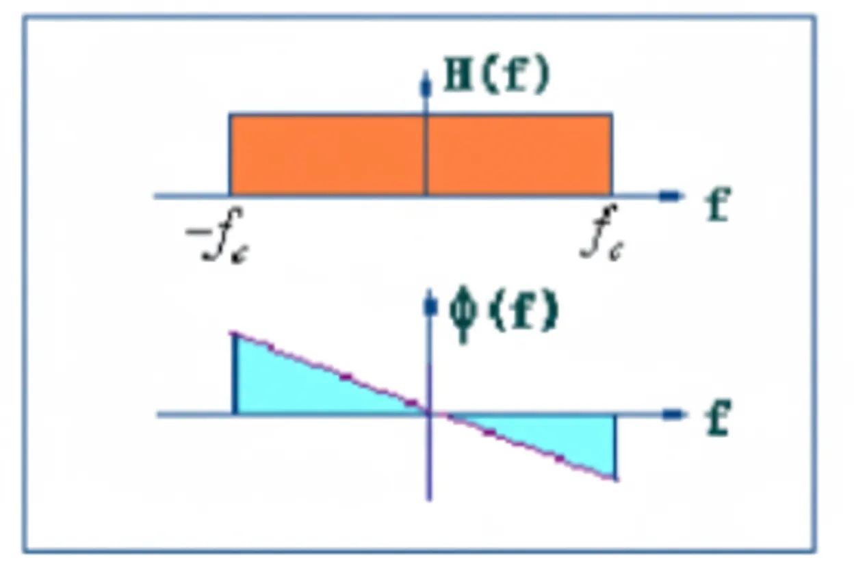
2.1 Ideal filter
An ideal filter would transmit signals in the passband without amplitude or phase distortion and attenuate stopband components to zero, with a sharp boundary between passband and stopband. In the passband the amplitude response would be constant and the phase slope constant; outside the passband the amplitude response would be zero.
2.2 Real filters
Ideal filters do not exist. In real filters there is no strict boundary between passband and stopband. A transition band exists where frequencies are attenuated rather than completely suppressed. Designers aim to make the transition band as narrow as possible to achieve faster attenuation outside the passband. Real filter design attempts to approximate the ideal response using various techniques.
3. Filter Technical Parameters
Key parameters include insertion loss, return loss, passband bandwidth, passband ripple, ripple, passband VSWR, center frequency, cutoff frequency, delay, and passband phase linearity.
3.1 Insertion loss
Insertion loss is the attenuation introduced by adding the filter to a circuit, typically specified at the center or cutoff frequency, or across the full band if required. It is defined as the ratio of the signal voltage from source to load without the filter to the signal voltage with the filter inserted:
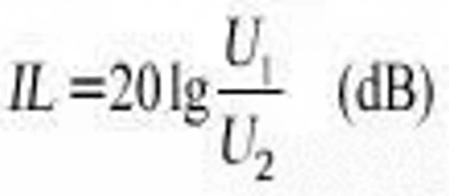
U1 — voltage at the load with no filter connected.
U2 — voltage at the load with the filter inserted.
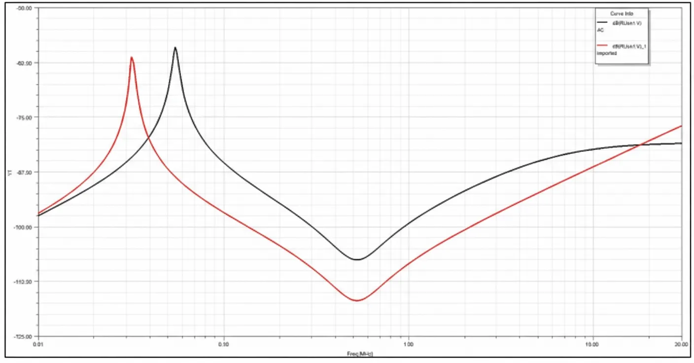
Insertion loss simulation curve
3.2 Return loss
Also called reflection loss, it indicates reflected power due to impedance mismatch.
Higher return loss is better to reduce reflected signals; when all input power is absorbed return loss is infinite.
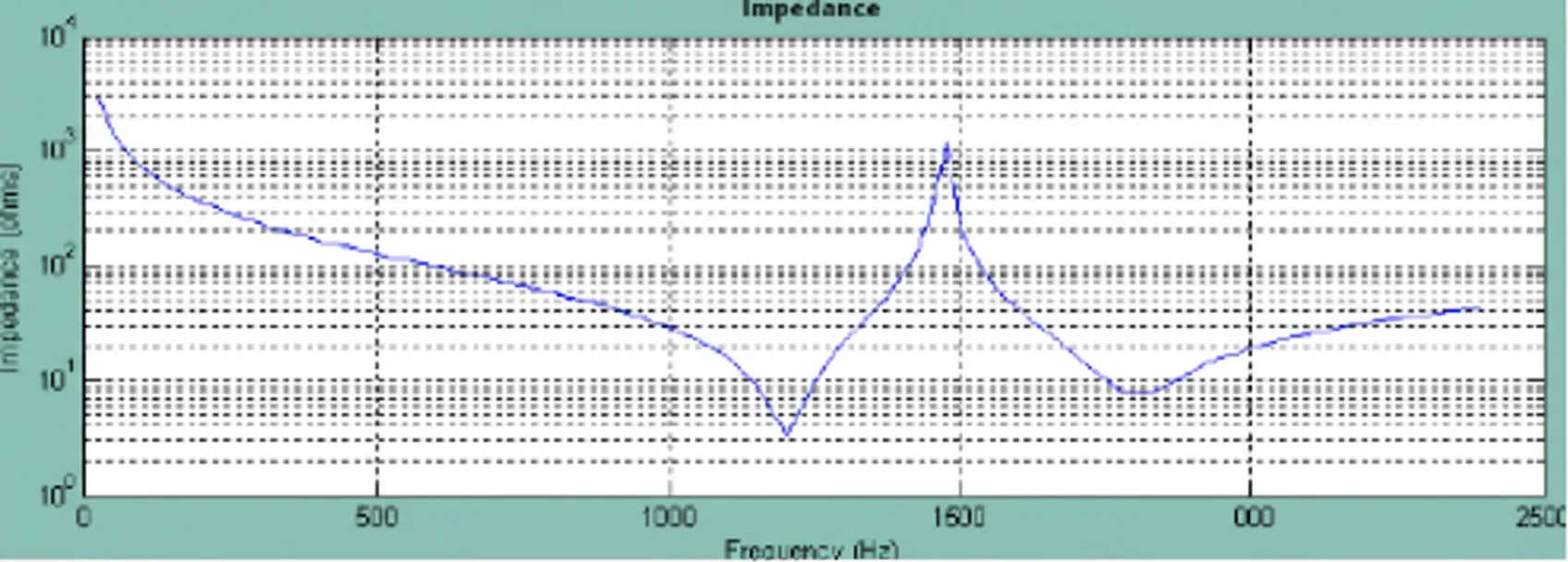
3.3 Impedance characteristics
Input and output impedances directly affect insertion loss. For EMI filters, maintain effective suppression under maximum expected impedance mismatch. Signal filters should match the source and load impedances for the desired signals to avoid attenuation. For unwanted signals or interference, maximize impedance mismatch to improve filtering.
Impedance simulation example:
Filter selection based on source and load impedances:
| Source impedance | Filter type | Load impedance |
|---|---|---|
| High | C, π, multi-stage π | High |
| High | Γ, multi-stage Γ | Low |
| Low | Inverse Γ, multi-stage inverse Γ | High |
| Low | L, T, multi-stage T | Low |
Filters must meet the operating and suppression frequency requirements of the load circuit. At the required frequencies the filter impedance must match the interfering source and load impedances. If the interference source is high impedance, the filter output should be low impedance; if the source is low impedance, the filter output should be high impedance.
3.4 Other parameters
3.4.1 Delay (TD)
The time required for a signal to pass through the filter, numerically the derivative of transmission phase with respect to angular frequency, TD = dΦ/dω.
3.4.2 Ripple
Peak-to-peak variation of insertion loss around the mean loss curve within the 3 dB bandwidth (cutoff frequency range).
3.4.3 Passband ripple
Variation of insertion loss within the passband. One-dB bandwidth has 1 dB of passband ripple.
3.4.4 Passband VSWR
A key metric for how well the filter matches the transmission within the passband. Ideal match VSWR = 1:1. When mismatched:
At points where incident and reflected waves are in phase, voltage amplitudes add to form a maximum VMAX (antinode). Where they are out of phase, they subtract to form a minimum VMIN (node). The standing wave ratio is VMAX/VMIN.
3.4.5 Passband phase linearity
This parameter characterizes phase distortion introduced in the passband. Filters designed for linear phase response have good phase linearity.
3.4.6 Cutoff frequency
For low-pass filters the right-edge passband frequency, and for high-pass filters the left-edge passband frequency, usually defined at relative loss points such as 1 dB or 3 dB. Reference loss is DC insertion loss for low-pass; for high-pass use insertion loss measured at a sufficiently high frequency where parasitic stopbands are not present.
3.4.7 Center frequency
The center frequency f0 of a filter passband is generally f0 = (f1 + f2)/2, where f1 and f2 are the left and right 1 dB or 3 dB edge frequencies for band-pass or band-stop filters. Narrowband filters often use the frequency of minimum insertion loss as the center frequency to compute bandwidth.
4. Filter Installation Requirements
4.1 Filter placement
- If one interference source affects multiple sensitive devices, place the filter close to the interference source. If there is one sensitive device and multiple interference sources, place the filter close to the sensitive device. Placing the filter near the interference source confines the disturbance locally and interrupts its emission path.
- On PCBs, install filters at interfaces. When multiple filters are needed, mount them in parallel to prevent coupling between signal lines before and after filtering. If an interface has a single interference source, mount the filter as close as possible to the source.
4.2 Wiring for filter input and output
- Input and output lines must be shielded and isolated. If input and output wiring are close together they can couple and reduce filtering effectiveness.
- Avoid routing other signal wiring near the lines that require additional filtering to prevent coupling from the interference source to other lines, which would reduce the filter's effectiveness.
- Routed, filtered signal traces should avoid proximity to strong interference lines to prevent secondary contamination of the filtered signals.
4.3 Grounding requirements
- Do not use a thin ground trace for the filter; at high frequency this provides poor filtering. Ensure the filter casing is well bonded to metal structure planes to improve grounding.
- Choose filter ground points on a quiet ground plane free from strong interference. Keep ground leads as short and wide as possible to reduce parasitic inductance, and locate the ground connection at a point that minimizes the return-loop area for interfering currents.