 ALLPCB


In the fast-evolving world of electronics manufacturing, advanced silkscreen techniques like multi-layer silkscreen printing are revolutionizing how complex electronic devices are designed and produced. If you're searching for ways to enhance precision and functionality in your electronic projects, multi-layer silkscreen, thick film printing, and even 3D silkscreen methods offer cutting-edge solutions. These techniques allow for intricate designs, improved durability, and better performance in devices ranging from wearable sensors to high-speed circuit boards.
In this comprehensive guide, we'll dive deep into the world of advanced printing techniques, focusing on multi-layer silkscreen for complex electronics. You'll learn what these methods are, how they work, and why they’re critical for modern electronic applications. Let’s explore how these innovations can elevate your next project with practical insights and technical details.
What Is Multi-Layer Silkscreen Printing?
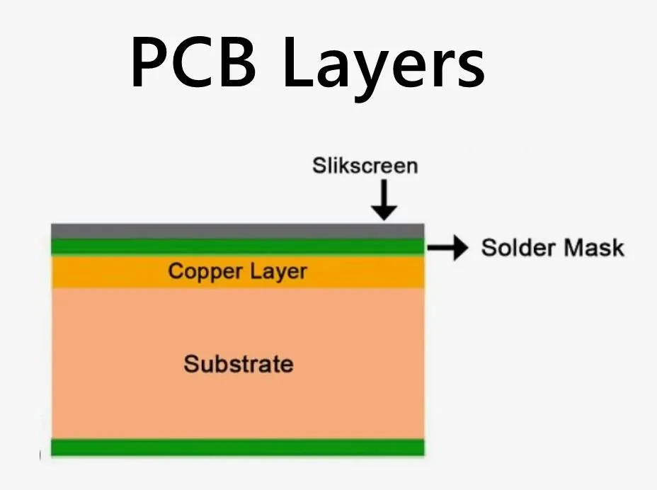
Multi-layer silkscreen printing is an advanced printing technique used in electronics manufacturing to apply multiple layers of ink or conductive materials onto a substrate, such as a printed circuit board (PCB). Unlike traditional single-layer silkscreening, which is often used for labeling or basic designs, multi-layer silkscreen builds up several layers to create complex patterns, protective coatings, or even functional components like resistors and capacitors directly on the board.
This method is especially valuable for complex electronics where space is limited, and high precision is required. By stacking layers of materials with different properties—such as insulating, conductive, or dielectric inks—manufacturers can achieve intricate designs that support high-density circuits and advanced functionalities. For instance, in a multi-layer PCB, silkscreen layers might be used to add identifying marks on the top layer while underlying layers integrate thick film printing for embedded components.
Why Multi-Layer Silkscreen Matters for Complex Electronics
Complex electronic devices, such as smartphones, medical sensors, and aerospace systems, demand compact designs with high performance. Multi-layer silkscreen printing meets these needs by enabling:
- Miniaturization: Multiple layers reduce the footprint of components, allowing more functionality in smaller spaces.
- Enhanced Durability: Protective layers shield sensitive components from environmental factors like moisture or heat.
- Cost Efficiency: Integrating components directly into layers reduces the need for separate parts, cutting assembly costs.
Advanced Printing Techniques in Electronics Manufacturing
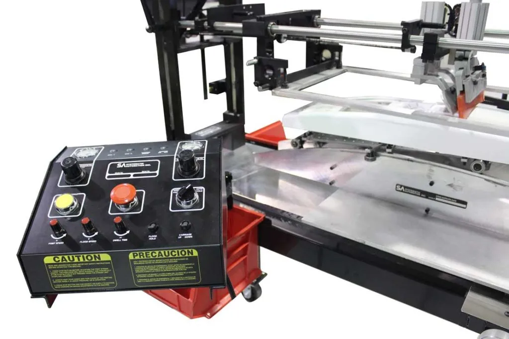
Beyond basic silkscreening, advanced printing techniques have emerged to tackle the challenges of modern electronics. These methods push the boundaries of precision and functionality, making them ideal for high-tech applications. Let’s break down some key approaches, including thick film printing and 3D silkscreen, alongside multi-layer methods.
Thick Film Printing for Robust Components
Thick film printing is a specialized silkscreen technique where thicker layers of conductive or resistive inks are applied to a substrate. This method is often used to create components like resistors, capacitors, and heaters directly on a circuit board or ceramic base. The “thick” aspect refers to the layer thickness, typically ranging from 10 to 50 micrometers, compared to thin film layers which are often below 1 micrometer.
In complex electronics, thick film printing is prized for its ability to handle high power and harsh conditions. For example, in automotive electronics, thick film resistors can withstand temperatures up to 150°C and maintain stable resistance values, ensuring reliable performance. This technique also supports multi-layer designs by allowing different materials to be stacked for hybrid circuits, combining passive and active components in one compact unit.
3D Silkscreen: Printing Beyond Flat Surfaces
Traditional silkscreen printing is limited to flat surfaces, but 3D silkscreen techniques break this barrier by enabling printing on curved or irregular shapes. This is achieved through advanced equipment and flexible screen materials that adapt to the geometry of the target surface. In the context of complex electronics, 3D silkscreen is a game-changer for wearable devices and IoT gadgets where components must conform to non-standard shapes.
For instance, 3D silkscreen can be used to print conductive traces directly onto the casing of a smartwatch, eliminating the need for a separate PCB in some areas. This not only saves space but also reduces weight, a critical factor in portable devices. Recent innovations, as noted in studies from scientific journals, highlight how 3D printing combined with silkscreen methods can achieve resolutions as fine as 100 micrometers, rivaling traditional manufacturing precision.
How Multi-Layer Silkscreen Enhances Complex Electronics
Multi-layer silkscreen printing is not just about aesthetics or labeling; it plays a functional role in the performance of complex electronic devices. By leveraging precise layering, this technique addresses critical challenges in signal integrity, thermal management, and component integration. Let’s explore specific ways it adds value.
Improved Signal Integrity with Layered Insulation
In high-speed electronics, maintaining signal integrity is paramount. Multi-layer silkscreen can apply insulating layers between conductive traces to minimize crosstalk and electromagnetic interference (EMI). For example, in a 5G communication module, silkscreened dielectric layers can separate signal lines, reducing impedance mismatches and ensuring signal speeds remain consistent at frequencies above 3 GHz.
These insulating layers, often made of polymer-based inks, can be tailored to specific dielectric constants (typically between 2.5 and 4.5), optimizing the board for high-frequency applications. This precision is vital for devices like radar systems or advanced wireless routers where even minor signal loss can degrade performance.
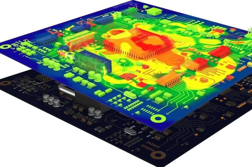
Thermal Management through Strategic Layering
Heat dissipation is a major concern in densely packed electronics. Multi-layer silkscreen can incorporate thermally conductive inks or coatings to draw heat away from critical components. For instance, a power management IC generating significant heat—sometimes exceeding 80°C during operation—can benefit from a silkscreened thermal layer that spreads heat evenly across the board.
This approach not only extends the lifespan of components but also prevents thermal hotspots that could cause failures. By integrating such layers during the printing process, manufacturers avoid the need for additional heat sinks or cooling solutions, streamlining the design.
Applications of Multi-Layer Silkscreen in Modern Devices
The versatility of multi-layer silkscreen printing makes it indispensable across various industries. From consumer gadgets to industrial systems, this technique supports innovation by enabling more efficient and reliable designs. Here are some key applications where it shines.
Wearable Electronics and Biosensors
Wearable devices, such as fitness trackers and medical biosensors, rely on compact, flexible designs. Multi-layer silkscreen printing allows for the integration of conductive traces, sensors, and protective coatings directly onto flexible substrates. This eliminates bulky connectors and reduces the overall thickness of the device, often to less than 0.5 mm.
For example, a heart rate sensor might use silkscreened silver ink for conductive paths and a protective polymer layer to shield against sweat and skin contact. The ability to print multiple layers ensures that functionality isn’t compromised, even in such a small form factor.
Aerospace and Automotive Systems
In aerospace and automotive applications, reliability under extreme conditions is non-negotiable. Multi-layer silkscreen, often combined with thick film printing, creates robust components that resist vibration, temperature swings, and humidity. A typical automotive control unit might use silkscreened thick film resistors with power ratings up to 5 watts, ensuring stable operation in engine compartments where temperatures can spike.
Moreover, multi-layer designs help reduce weight and space, critical factors in aircraft and electric vehicles where every gram counts. The precision of advanced printing techniques also supports the high-density wiring needed for modern avionics and autonomous driving systems.
Challenges and Future Trends in Advanced Silkscreen Techniques
While multi-layer silkscreen and related methods offer immense benefits, they come with challenges that manufacturers must address. Understanding these hurdles and upcoming trends can help engineers stay ahead in the field of complex electronics.
Challenges in Precision and Material Compatibility
One of the main challenges in multi-layer silkscreen printing is achieving uniform layer thickness and alignment across multiple passes. Misalignment by even 10 micrometers can lead to short circuits or signal degradation in high-density designs. Additionally, ensuring compatibility between different inks—such as conductive and insulating materials—requires careful formulation to prevent cracking or delamination during curing.
Manufacturers are tackling these issues with automated printing systems equipped with high-resolution imaging to detect and correct misalignments in real-time. Advances in ink chemistry are also improving adhesion and flexibility, especially for 3D silkscreen applications on unconventional surfaces.
Emerging Innovations: Smart Inks and Hybrid Printing
The future of advanced silkscreen techniques lies in smart materials and hybrid approaches. Smart inks, which change properties based on environmental conditions (like temperature or pressure), are being developed for self-monitoring electronics. Imagine a PCB with a silkscreened layer that changes color to indicate overheating—such innovations could transform maintenance in industrial systems.
Hybrid printing, combining silkscreen with other additive manufacturing methods like inkjet or electrohydrodynamic printing, is also gaining traction. Recent studies, such as those published in scientific journals, show that hybrid methods can achieve feature sizes as small as 70 nanometers, opening doors to next-generation microelectronics.
How to Implement Multi-Layer Silkscreen in Your Projects
If you’re an engineer or designer looking to leverage multi-layer silkscreen for your next project, start with these practical steps to ensure success.
- Define Your Requirements: Identify the specific needs of your device, such as signal frequency, thermal load, or form factor, to choose the right materials and layer configurations.
- Partner with Experts: Work with a trusted manufacturing service that specializes in advanced printing techniques to access the latest equipment and expertise.
- Test Iteratively: Prototype and test your designs under real-world conditions to validate performance, especially for high-stakes applications like medical or aerospace devices.
- Stay Updated: Keep an eye on industry advancements in materials and methods to incorporate cutting-edge solutions into your workflow.
By focusing on precision and collaboration, you can harness the power of multi-layer silkscreen to create complex electronics that stand out in performance and reliability.
Conclusion: Elevating Electronics with Advanced Silkscreen Techniques
Advanced silkscreen techniques like multi-layer printing, thick film printing, and 3D silkscreen are transforming the landscape of complex electronics. These methods enable smaller, more efficient, and more durable devices, meeting the demands of modern industries from wearables to aerospace. By understanding and applying these approaches, engineers can push the limits of innovation, creating products that excel in performance and design.
Whether you’re working on a high-speed communication module or a flexible biosensor, multi-layer silkscreen offers the precision and versatility needed to succeed. As technology continues to evolve with smart inks and hybrid printing, the possibilities for complex electronics are endless. Embrace these advanced printing techniques to stay ahead in the competitive world of electronics manufacturing.


