ALLPCB


ADS1118 is a high-precision, low-power, 16-bit analog-to-digital converter (ADC) that integrates the functions needed to measure common sensor signals. It is available in a very small X2QFN-10 package or a VSSOP-10 package. The ADS1118 integrates a programmable-gain amplifier (PGA), voltage reference, oscillator, and a high-accuracy temperature sensor. With a wide supply range from 2 V to 5.5 V, the ADS1118 is suitable for sensor measurement applications with constraints on power and board area.
The ADS1118 supports data conversion rates up to 860 samples per second (SPS). The PGA provides input ranges from ±256 mV to ±6.144 V, enabling high-resolution measurement of both small and large signals. An input multiplexer (MUX) supports two differential inputs or four single-ended inputs. The integrated temperature sensor can be used for system-level temperature monitoring or cold-junction compensation for thermocouples.
The ADS1118 can operate in continuous-conversion mode or single-shot mode, with automatic power-down after conversion in single-shot mode to reduce idle current. Data is transmitted via a serial peripheral interface (SPI). The specified operating temperature range is ?40°C to +125°C.
Features
- Very small X2QFN package: 2.0 mm × 1.5 mm × 0.4 mm
- Wide supply range: 2 V to 5.5 V
- Low current consumption:
- Continuous mode: typical 150 μA
- Single-shot mode: automatic power-down
- Programmable data rates: 8 SPS to 860 SPS
- Single-cycle settling
- Internal low-drift voltage reference
- Integrated temperature sensor: 0.5°C maximum error from 0°C to 70°C
- Internal oscillator
- Integrated PGA
- Four single-ended or two differential inputs
Block Diagram
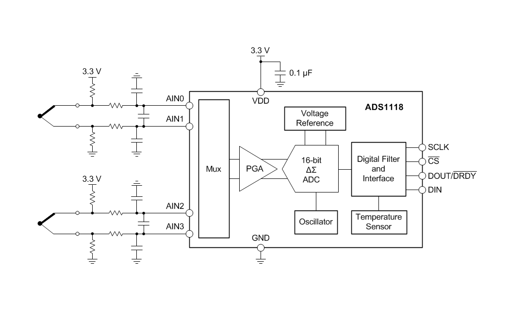
The ADS1118 is a highly integrated 16-bit delta-sigma ADC from TI that includes a programmable-gain amplifier (PGA), internal reference, oscillator, and a high-accuracy temperature sensor. It uses an SPI interface for communication and supports a 2 V to 5.5 V supply. Typical application areas include temperature measurement for thermocouples and thermistors, portable instruments, and industrial control where low power and small size are required.
1. Device Overview and Key Characteristics
1.1 Basic Specifications
- Document and packages: Document number SBAS457F, published October 2010 and revised September 2019. Two package options: 10-pin X2QFN (1.5 mm × 2.0 mm) and 10-pin VSSOP (3.0 mm × 3.0 mm). Both are lead-free. MSL rating: 1 (X2QFN) / 2 (VSSOP). Peak reflow temperature 260°C.
- Supply and temperature: Supply voltage 2 V to 5.5 V; absolute maximum 7 V. Operating temperature ?40°C to 125°C; maximum junction temperature 150°C. Thermal resistance junction-to-ambient: 245.2°C/W (X2QFN), 186.8°C/W (VSSOP). ESD protection: HBM ±4000 V, CDM ±1000 V. RoHS compliant.
- Pin functions: Analog inputs AIN0–AIN3, SPI pins SCLK/CS/DIN/DOUT/DRDY, VDD and GND. The DOUT/DRDY pin is multiplexed for data output and data-ready, active low.
1.2 Core Performance
- ADC performance: 16-bit resolution with no missing codes. Programmable rates from 8 SPS to 860 SPS. PGA supports six full-scale ranges (FSR) from ±256 mV to ±6.144 V; the smallest LSB is 7.8125 μV for the ±256 mV range. Integral nonlinearity (INL) ±1 LSB. Gain error up to 0.15%, offset error up to ±2 LSB.
- Temperature sensor: Measurement range ?40°C to 125°C. Resolution 0.03125°C per LSB. Accuracy ±0.5°C from 0°C to 70°C, ±1°C over the full range. Supports cold-junction compensation.
- Power and noise: Continuous mode typical 150 μA (3.3 V, 8 SPS). Power-down mode 0.5 μA. Input-referred noise down to 7.81 μVrms (±256 mV range, 8 SPS). Common-mode rejection ratio (CMRR) up to 105 dB.
2. Key Functions and Operating Principles
2.1 Core Functions
- Signal acquisition and amplification:
- Supports four single-ended inputs or two differential inputs selectable via the input multiplexer (MUX). Differential mode suppresses common-mode noise. In single-ended mode, the negative inputs are internally tied to ground.
- PGA gain is programmable to accommodate different sensor amplitudes. Use higher gain for small signals such as thermocouples and lower gain for large signals to avoid saturation.
- Operating modes and low power:
- Supports continuous-conversion mode and single-shot mode. Continuous mode continuously samples and updates results. Single-shot mode completes a conversion then powers down to reduce idle power. Periodic single-shot triggering can optimize power through duty cycling.
- The device defaults to power-down and must be configured via SPI to start conversions. Lower sampling rates reduce noise and power consumption; 8 SPS yields the lowest noise while 860 SPS yields the fastest response.
- Temperature measurement and calibration:
- The internal temperature sensor can operate independently. Enabling temperature mode via the configuration register returns a 14-bit left-aligned result in two's complement format for negative temperatures.
- The internal reference is integrated and not user-replaceable. Reference error and drift are included in the device gain error and drift specifications. The configuration register can be read over SPI to verify operating parameters.
2.2 Operating Principle
- Analog signals applied to AIN0–AIN3 are selected by the MUX as single-ended or differential inputs and routed to the PGA. The amplified signal is converted by a delta-sigma modulator into a high-rate bit stream, which is digitally filtered and decimated to yield a 16-bit result stored in the conversion register.
- The SPI interface uses mode 1 (CPOL=0, CPHA=1). Transfers can be 16 bits (read conversion result only) or 32 bits (read conversion result plus read back configuration register). The DOUT/DRDY pin goes low when conversion completes to indicate data ready and can trigger a host read.
- In temperature mode, the internal temperature sensor output is converted and output via SPI. Conversion formulas: temperature = code × 0.03125°C for nonnegative values, or temperature = ?(65536 ? code) × 0.03125°C for negative values.
3. Applications and Design Recommendations
3.1 Typical Applications
- Temperature measurement: Cold-junction compensation for thermocouples, thermistor signal acquisition, and ambient temperature monitoring using the integrated temperature sensor to reduce external components.
- Industrial control: Analog signal acquisition in factory automation such as pressure and flow sensors. Differential input mode offers good noise immunity in industrial environments.
- Portable equipment: Low-power data acquisition modules for notebooks and handheld instruments. Single-shot mode with automatic power-down extends battery life.
3.2 Design Considerations
- Input and gain configuration:
- For differential inputs, match source impedances to preserve linearity. For single-ended inputs, input voltage must remain within 0 V to VDD. Exceeding the supply may forward-bias ESD protection diodes.
- Select the FSR according to sensor output amplitude. For millivolt-level signals such as thermocouples, use ±256 mV or ±512 mV ranges. For larger signals up to 0–5 V, use the ±6.144 V range to avoid saturation while maintaining resolution.
- SPI communication and timing:
- CS is active low; when not used it can be pulled high. A low SCLK held for more than 28 ms resets the SPI interface, so avoid communication interruptions that assert SCLK low for extended periods.
- After data-ready, complete the read before DOUT/DRDY is released. In continuous mode, DOUT/DRDY will be released 8 μs before the next conversion.
- Layout and power:
- Connect analog and digital grounds at a single point. Route analog inputs away from digital circuits and switching noise sources. Unused AIN pins may be tied to VDD or left floating as recommended to avoid injecting noise.
- Place a 0.1 μF decoupling capacitor close to VDD. Use a stable supply to avoid noise affecting conversion accuracy; in wide-voltage applications consider using an LDO regulator.
- Anti-alias filtering:
- Add an RC low-pass filter on analog inputs. Set the filter cutoff to within about 10 times the sampling rate to suppress signals above the Nyquist frequency. Use resistor values below 1 kΩ to avoid introducing additional offset errors.
4. Key Configuration Points
- Range and data rate: Select FSR via PGA[2:0] bits in the configuration register and data rate via DR[2:0] bits. Lower data rates (8 SPS–64 SPS) are suited to high-precision measurements; higher rates (250 SPS–860 SPS) support fast response.
- Operating mode: MODE bit selects continuous mode (0) or single-shot mode (1). In single-shot mode, trigger a conversion via the SS bit; the device powers down after conversion. Continuous mode offers continuous updates but higher power consumption.
- Channel and temperature mode: MUX[2:0] selects input channel (single-ended or differential). TS_MODE bit selects ADC mode (0) or temperature sensor mode (1). Temperature measurements and signal acquisition can be alternated.