 ALLPCB


In the fast-evolving world of electronics, High-Density Interconnect (HDI) PCB design is at the forefront of innovation, enabling smaller, faster, and more powerful devices. A critical factor in achieving success with HDI PCBs is precision in imaging techniques. But what exactly is HDI PCB imaging, and how does it impact fine-line PCB manufacturing? Simply put, HDI PCB imaging involves advanced methods like laser direct imaging to create intricate circuit patterns with exceptional accuracy, ensuring high-density designs meet strict performance standards.
In this comprehensive guide, we’ll dive deep into the role of imaging in HDI PCB manufacturing. From the basics of fine-line PCB production to the cutting-edge use of laser direct imaging for HDI, we’ll explore how advanced PCB resolution and high-accuracy PCB pattern transfer shape the future of electronics. Whether you’re an engineer, designer, or tech enthusiast, this blog will equip you with valuable insights into achieving precision in your projects.
What is HDI PCB Imaging and Why Does It Matter?
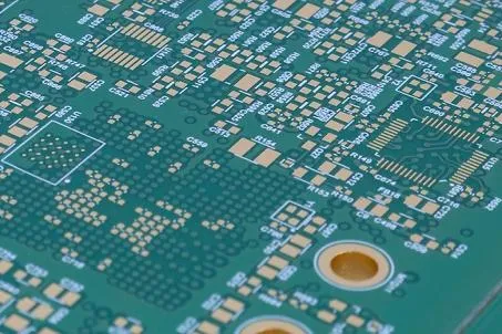
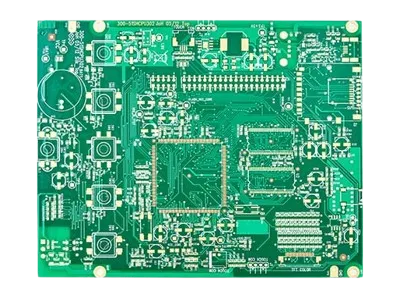
High-Density Interconnect (HDI) PCBs are specialized circuit boards designed to pack more functionality into smaller spaces. They feature finer lines, smaller vias (often microvias), and higher layer counts compared to traditional PCBs. To achieve this level of complexity, HDI PCB imaging plays a pivotal role. Imaging is the process of transferring circuit patterns onto the PCB substrate with extreme precision, ensuring that every trace and connection aligns perfectly.
Without advanced imaging techniques, creating the fine lines and tight tolerances required for HDI designs—often as narrow as 50 micrometers (μm) or less—would be impossible. Poor imaging can lead to signal integrity issues, crosstalk, or even complete board failure. By leveraging cutting-edge methods like laser direct imaging for HDI, manufacturers can achieve the high-accuracy PCB pattern transfer needed for reliable performance in applications like smartphones, medical devices, and automotive systems.
The Challenges of Fine-Line PCB Manufacturing
Fine-line PCB manufacturing is the backbone of HDI technology, focusing on creating circuit traces and spaces that are incredibly narrow, often below 75 μm. This level of miniaturization is essential for modern electronics but comes with significant challenges:
- Tight Tolerances: Even a slight misalignment in pattern transfer can disrupt signal flow, especially in high-speed designs where impedance control is critical (e.g., maintaining 50 ohms for RF signals).
- Material Constraints: The substrates used in HDI designs, such as thin laminates, are more prone to warping or defects during imaging and etching.
- Signal Integrity: Narrow traces and dense layouts increase the risk of interference and signal loss, demanding flawless imaging to maintain performance at speeds exceeding 10 Gbps in some applications.
Traditional imaging methods, like photolithography with film masks, often struggle to meet these demands due to limitations in resolution and alignment accuracy. This is where advanced techniques come into play, revolutionizing the way fine-line PCBs are manufactured.
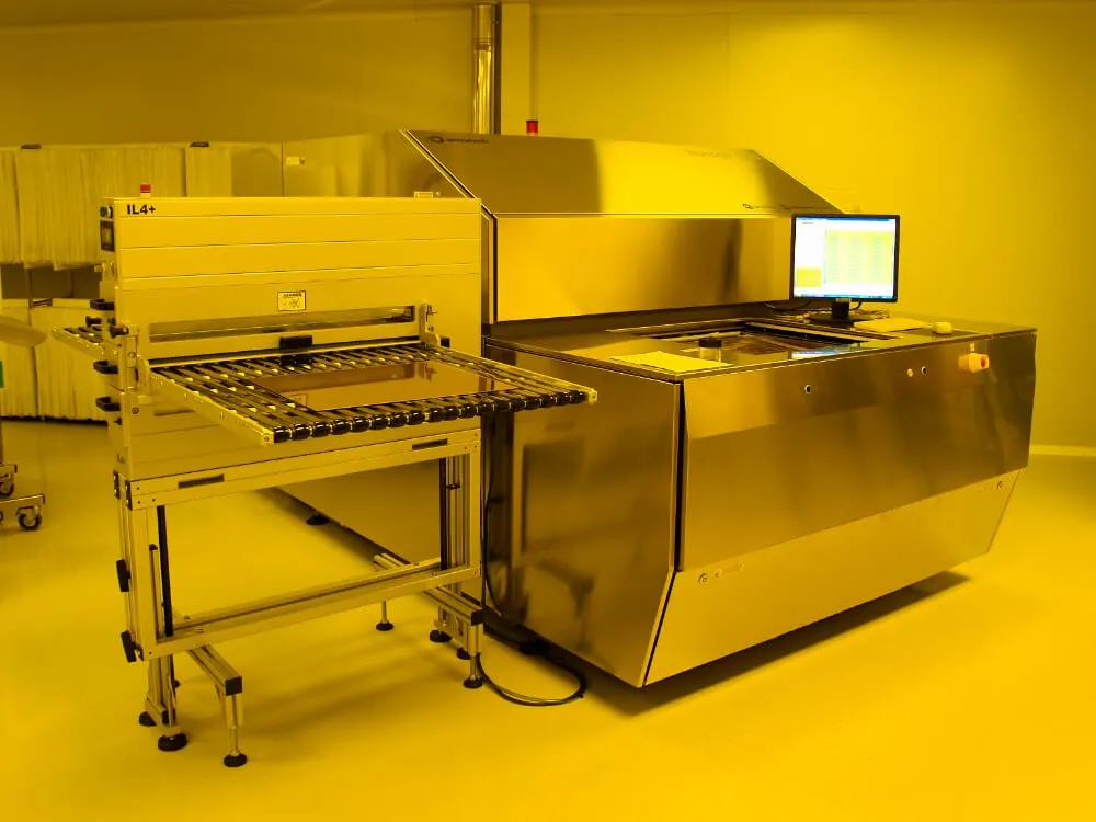
Laser Direct Imaging for HDI: A Game-Changer
Laser Direct Imaging (LDI) is a modern imaging technology that has transformed HDI PCB production. Unlike conventional methods that rely on physical masks, LDI uses a laser to directly write circuit patterns onto the photoresist layer of the PCB. This approach offers several advantages for achieving advanced PCB resolution and high-accuracy PCB pattern transfer:
- Sub-Micron Precision: LDI systems can achieve resolutions finer than 25 μm, making them ideal for the intricate patterns required in HDI designs.
- Elimination of Masks: By removing the need for physical masks, LDI reduces errors caused by mask misalignment and cuts production time.
- Flexibility: LDI allows for quick design changes without the need to create new masks, speeding up prototyping and production cycles.
In practical terms, LDI ensures that trace widths and spacing remain consistent, even in densely packed areas of the board. For instance, in a multilayer HDI PCB with 6 layers, LDI can maintain alignment accuracy within 10 μm across all layers, minimizing registration errors that could disrupt via connections.
Advanced PCB Resolution: Pushing the Boundaries
Resolution in PCB imaging refers to the ability to create clear, distinct patterns at the smallest possible scale. Advanced PCB resolution is critical for HDI designs, where every micrometer counts. With traditional imaging, resolution is often limited by the quality of the mask and the exposure process, leading to blurred edges or uneven traces.
Modern imaging technologies, particularly LDI, overcome these limitations by using focused laser beams to achieve sharp, clean lines. Some systems can produce resolutions as fine as 15 μm, allowing for trace widths and spaces that support high-speed signals without interference. This level of detail is essential for applications like 5G devices, where signal integrity at frequencies above 28 GHz depends on precise trace geometry.
Moreover, advanced resolution isn’t just about smaller lines—it’s also about consistency. High-resolution imaging ensures that every trace on the board matches the design specifications, reducing the risk of defects that could lead to costly rework or product failures.
High-Accuracy PCB Pattern Transfer: Ensuring Reliability
Pattern transfer is the process of moving the circuit design from the imaging stage to the physical board through etching or other methods. High-accuracy PCB pattern transfer is non-negotiable in HDI manufacturing, as even a small deviation can cause short circuits or open connections in densely packed layouts.
In traditional processes, pattern transfer often suffers from issues like under-etching or over-etching, where the etchant removes too little or too much copper, respectively. Advanced imaging techniques paired with precise control systems minimize these risks. For example, LDI not only creates accurate patterns but also integrates with automated alignment tools to ensure that the pattern transfers perfectly onto each layer of a multilayer HDI board.
The result? Boards that meet stringent quality standards, with trace widths maintained within ±5 μm of the intended design. This level of accuracy is vital for ensuring reliability in critical applications, such as medical implants operating at low power levels (e.g., 1.8V) where any signal disruption could be catastrophic.
Benefits of Precision Imaging in HDI PCB Design
The impact of precision imaging on HDI PCB design extends beyond technical accuracy—it delivers tangible benefits for manufacturers and end-users alike. Here are some key advantages:
- Smaller Form Factors: Precision imaging enables tighter trace spacing and smaller vias, allowing designers to shrink board sizes without sacrificing functionality. For example, HDI boards in smartphones can reduce footprint by up to 30% compared to standard PCBs.
- Enhanced Performance: Accurate pattern transfer and high resolution minimize signal loss and crosstalk, supporting high-speed data transfer rates above 25 Gbps in advanced computing systems.
- Cost Efficiency: While advanced imaging technologies require upfront investment, they reduce errors and rework, ultimately lowering production costs. LDI, for instance, can cut prototyping lead times by 50% or more by eliminating mask production.
- Reliability in Harsh Environments: HDI PCBs with precise imaging are better equipped to handle thermal and mechanical stress, making them ideal for automotive and aerospace applications where temperatures can exceed 125°C.
Applications of HDI PCB Imaging in Modern Electronics
The precision enabled by advanced imaging techniques has opened doors to a wide range of applications for HDI PCBs. Some notable examples include:
- Consumer Electronics: Smartphones, tablets, and wearables rely on HDI PCBs to fit complex circuitry into compact designs. Imaging precision ensures that these devices maintain performance despite their small size.
- Medical Devices: Implantable devices like pacemakers use HDI PCBs with microvias as small as 50 μm in diameter, requiring flawless imaging to ensure patient safety.
- Automotive Systems: Advanced driver-assistance systems (ADAS) depend on HDI PCBs for high-speed signal processing, with imaging accuracy ensuring reliable operation under varying conditions.
- Telecommunications: 5G infrastructure demands HDI boards capable of handling high-frequency signals, where imaging precision directly impacts network performance.
How to Choose the Right Imaging Technology for Your HDI PCB Project
Selecting the appropriate imaging technology for your HDI PCB project depends on several factors, including design complexity, production volume, and budget. Here are some considerations to guide your decision:
- Design Requirements: If your project involves trace widths below 50 μm or multilayer boards with microvias, laser direct imaging for HDI is likely the best choice due to its superior resolution.
- Production Scale: For high-volume runs, investing in advanced imaging systems can save time and reduce defects, while smaller batches might justify traditional methods if tolerances are less strict.
- Turnaround Time: Technologies like LDI offer faster prototyping by eliminating mask creation, which is ideal for projects with tight deadlines.
- Budget Constraints: While advanced imaging delivers unmatched precision, it comes at a higher initial cost. Weigh the benefits of reduced rework against upfront expenses.
Partnering with a manufacturer that offers state-of-the-art imaging capabilities can also streamline the process, ensuring your HDI designs meet the highest standards of quality and performance.
Future Trends in HDI PCB Imaging
The field of HDI PCB imaging is continuously evolving, driven by the demand for even smaller, faster, and more efficient electronics. Some emerging trends to watch include:
- AI-Driven Imaging: Artificial intelligence is being integrated into imaging systems to optimize pattern transfer, predict defects, and enhance resolution beyond current limits.
- Next-Generation Lasers: Developments in laser technology promise even finer resolutions, potentially reaching below 10 μm for ultra-dense HDI designs.
- Sustainable Processes: Manufacturers are exploring eco-friendly imaging solutions, such as reducing chemical usage in photoresist development, to align with global sustainability goals.
These advancements will further push the boundaries of what’s possible in fine-line PCB manufacturing, opening new opportunities for innovation across industries.
Conclusion: Precision as the Foundation of HDI Success
In the realm of High-Density Interconnect PCB design, precision is everything. HDI PCB imaging, powered by technologies like laser direct imaging for HDI, is the key to unlocking the full potential of fine-line PCB manufacturing. By achieving advanced PCB resolution and high-accuracy PCB pattern transfer, manufacturers can create boards that meet the stringent demands of modern electronics, from compact consumer gadgets to life-saving medical equipment.
Understanding and leveraging these imaging techniques is essential for staying ahead in a competitive industry. Whether you’re designing a multilayer board for a 5G application or prototyping a wearable device, precision imaging ensures your project succeeds from concept to production. With ongoing advancements in technology, the future of HDI PCB imaging promises even greater possibilities, paving the way for the next generation of electronic innovation.


