ALLPCB


If you're an electronics engineer looking to understand the ins and outs of white silkscreen on PCBs, you're in the right place. White silkscreen is a popular choice in PCB design for labeling and marking components, offering clear visibility and aiding in assembly and troubleshooting. In this guide, we'll dive deep into white silkscreen PCB design, manufacturing, assembly, troubleshooting, and cost considerations to help you make informed decisions for your projects.
At ALLPCB, we’re committed to providing you with the knowledge and tools to optimize your PCB projects. Whether you're designing a new board or refining an existing one, this comprehensive guide will walk you through every aspect of using white silkscreen effectively. Let's get started!
What Is White Silkscreen on PCBs?
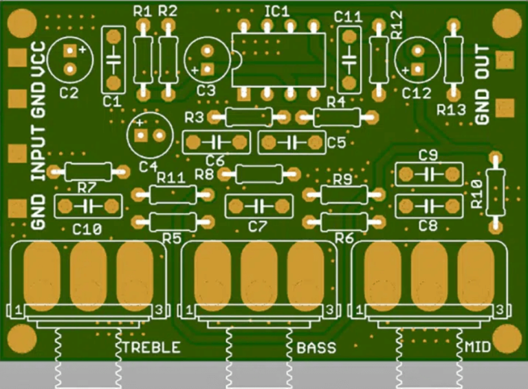
White silkscreen, often referred to as "legend printing," is a layer of ink applied to the surface of a printed circuit board (PCB) to display text and symbols. This layer typically includes component designators (like R1 for a resistor), polarity markers, pin numbers, test points, and other critical information. The white color is widely used due to its high contrast against most PCB solder mask colors, such as green, blue, or black, making it easy to read during assembly and maintenance.
The silkscreen layer is not just decorative—it’s a functional part of the PCB that helps engineers and technicians identify components and troubleshoot issues. By using white silkscreen, you ensure that markings are legible even in low-light conditions or on densely populated boards. Now, let’s explore how white silkscreen plays a role in various stages of PCB development.
White Silkscreen PCB Design: Key Considerations
Designing a PCB with white silkscreen requires careful planning to ensure clarity and functionality. Here are some essential tips for incorporating white silkscreen into your PCB design:
- Font Size and Style: Use a font size of at least 6 points (about 0.8 mm in height) to ensure readability. Avoid overly complex fonts—stick to simple, sans-serif styles like Arial for maximum clarity.
- Placement: Position silkscreen markings near the corresponding components without overlapping pads or vias. For densely packed boards, prioritize critical markings like polarity indicators over less essential ones.
- Contrast: White silkscreen works best on darker solder mask colors. If your board uses a light-colored mask, consider alternative silkscreen colors for better visibility.
- Orientation: Ensure text is oriented consistently, typically readable from a single angle (e.g., left to right), to avoid confusion during assembly.
By following these design principles, you can create a PCB layout that not only looks professional but also supports efficient assembly and debugging processes. Remember that the design phase sets the foundation for manufacturing, so precision is key.
White Silkscreen PCB Manufacturing: Process and Techniques
The manufacturing of white silkscreen on PCBs involves applying a layer of ink to the board’s surface using specialized techniques. Understanding this process can help you optimize your design for production. Here’s how it works:
- Preparation: After the PCB’s copper layers and solder mask are applied, the board is prepared for silkscreen printing. This involves cleaning the surface to ensure proper ink adhesion.
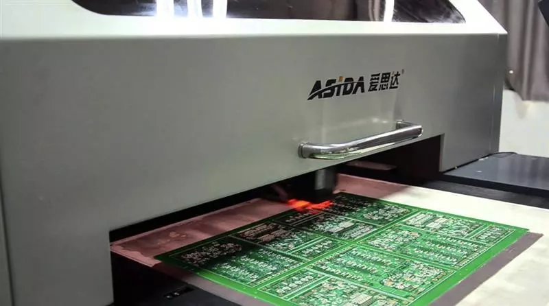
- Printing Method: There are three common methods for applying white silkscreen:
- Manual Screen Printing: Suitable for low-volume production, this traditional method uses a mesh screen to apply ink. It’s cost-effective but less precise for intricate designs.
- Liquid Photo Imaging (LPI): This advanced method uses a photosensitive ink exposed to UV light for high precision, ideal for complex or fine markings.
- Direct Legend Printing (DLP): A digital printing technique that offers flexibility and accuracy, often used for prototypes or small batches.
- Curing: Once the white ink is applied, it’s cured using heat or UV light to ensure durability against handling and environmental factors.
Choosing the right manufacturing method depends on your project’s complexity and volume. For high-density designs, LPI or DLP methods are recommended to achieve the precision needed for small text and symbols. At ALLPCB, we offer advanced manufacturing capabilities to ensure your white silkscreen is applied with the highest quality standards.
White Silkscreen PCB Assembly: Enhancing Efficiency
During PCB assembly, white silkscreen plays a critical role in guiding technicians through component placement and soldering. Here’s how it contributes to a smooth assembly process:
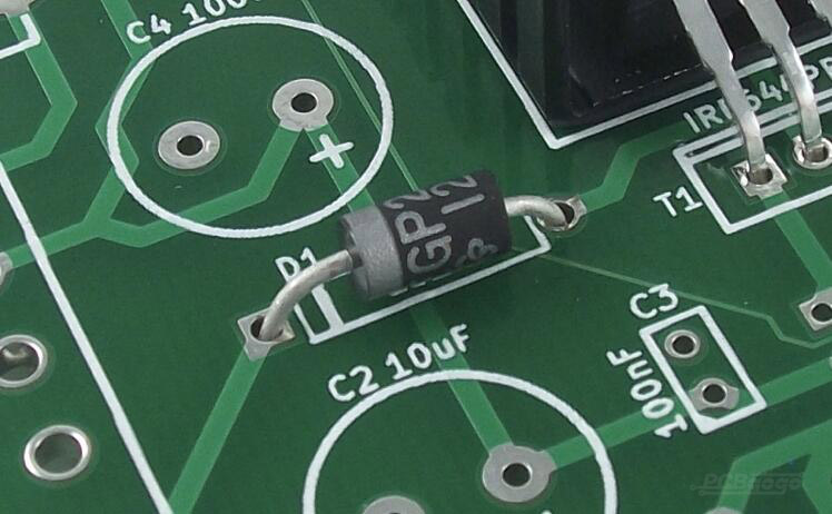
- Component Identification: White silkscreen labels like "C1" for a capacitor or "D1" for a diode help assemblers quickly locate and place components, reducing errors.
- Polarity Guidance: For components like diodes and electrolytic capacitors, polarity markers in white silkscreen prevent incorrect orientation, which could damage the board.
- Test Points: White silkscreen often marks test points (e.g., "TP1") for easy access during quality checks or debugging.
A well-designed white silkscreen layer can significantly speed up the assembly process, especially for manual assembly or when working with complex boards. For automated assembly lines, clear markings also assist in programming pick-and-place machines by providing visual references for component locations.
White Silkscreen PCB Troubleshooting: Simplifying Diagnostics
Troubleshooting a PCB can be a daunting task, especially on boards with hundreds of components. White silkscreen markings simplify this process by providing clear, readable information. Here’s how they help:
- Locating Components: During fault diagnosis, white silkscreen labels allow engineers to quickly find specific components or circuits, such as a failing resistor labeled "R5."
- Identifying Test Points: Test points marked with white silkscreen enable precise measurements of voltage or current, helping to pinpoint issues like short circuits or open connections.
- Pin Configuration: For ICs and connectors, white silkscreen often indicates pin 1 or other key pins, ensuring correct probing during testing.
For example, if a circuit isn’t functioning as expected, an engineer can use the white silkscreen to trace a signal path from a labeled input to an output, checking each marked component along the way. This visual aid reduces diagnostic time and minimizes the risk of errors.
White Silkscreen PCB Cost: Factors to Consider
Cost is always a concern in PCB production, and the use of white silkscreen can impact your budget. While silkscreening is generally a small portion of the overall cost, several factors influence the price:
- Board Complexity: More intricate designs with dense markings or smaller text require advanced printing methods like LPI or DLP, which can increase costs by 5-10% compared to manual screen printing.
- Volume: High-volume production often reduces the per-unit cost of silkscreening. For small runs or prototypes, expect to pay a setup fee that can range from $10 to $50 depending on the manufacturer.
- Color and Material: White silkscreen ink is typically standard and doesn’t add extra cost compared to other colors like yellow or black. However, custom ink formulations for specific durability requirements may raise costs slightly.
- Double-Sided Silkscreen: If you need white silkscreen on both sides of the PCB, this can increase costs by 10-20% due to additional processing steps.
On average, silkscreening adds about $0.10 to $0.50 per board for standard designs in medium to high volumes. For precise budgeting, it’s best to consult with your PCB provider to get a tailored quote based on your design specifications. At ALLPCB, we strive to offer competitive pricing while maintaining top-quality silkscreen application.
Best Practices for Using White Silkscreen on PCBs
To maximize the benefits of white silkscreen in your PCB projects, follow these best practices:
- Prioritize Critical Information: Focus on labeling essential elements like polarity markers and test points over decorative elements like logos if space is limited.
- Avoid Overcrowding: Too many markings can clutter the board and reduce readability. Use only necessary labels on densely populated PCBs.
- Test Readability: Before finalizing your design, print a prototype or use design software to simulate how the white silkscreen will look against your solder mask color.
- Collaborate with Manufacturers: Work closely with your PCB provider to ensure your silkscreen design meets their manufacturing capabilities and avoids potential issues like ink bleeding or misalignment.
By adhering to these guidelines, you can ensure that your white silkscreen not only looks professional but also serves its practical purpose effectively.
Common Issues with White Silkscreen and How to Avoid Them
While white silkscreen is highly beneficial, there are some common issues that can arise during design or manufacturing. Here’s how to address them:
- Ink Smudging or Fading: This can occur if the ink isn’t properly cured or if low-quality materials are used. Ensure your manufacturer uses high-quality ink and follows proper curing processes.
- Misalignment: Silkscreen text that isn’t aligned with components can cause confusion. Double-check your design files and provide clear instructions to the manufacturer.
- Poor Contrast: If white silkscreen appears faint on a light-colored solder mask, consider switching to a darker mask or a different silkscreen color for better visibility.
Proactive communication with your PCB provider can help mitigate these issues, ensuring a high-quality result for your boards.
Why Choose White Silkscreen for Your PCB Projects?
White silkscreen offers several advantages that make it a preferred choice for many electronics engineers:
- High Visibility: White ink stands out against most PCB backgrounds, making it easy to read under various lighting conditions.
- Versatility: It works well for a wide range of applications, from consumer electronics to industrial equipment.
- Cost-Effectiveness: White silkscreen is a standard option that doesn’t typically incur additional costs compared to other colors.
Whether you’re working on a prototype or a large-scale production run, white silkscreen provides a reliable way to enhance the functionality and professionalism of your PCBs.
Conclusion: Mastering White Silkscreen for PCB Success
White silkscreen on PCBs is more than just a labeling tool—it’s a critical element that supports every stage of a PCB’s lifecycle, from design and manufacturing to assembly and troubleshooting. By understanding the nuances of white silkscreen PCB design, manufacturing techniques, assembly benefits, troubleshooting aids, and cost factors, you can make informed decisions that elevate the quality of your projects.
At ALLPCB, we’re dedicated to helping electronics engineers like you achieve outstanding results with your PCB designs. Whether you’re incorporating white silkscreen for the first time or refining an existing design, our expertise and advanced manufacturing capabilities ensure your boards meet the highest standards. Start optimizing your PCB projects today with the power of white silkscreen!