 ALLPCB


In the world of advanced medical imaging, CT scanners stand out for their precision and speed in diagnosing health conditions. At the heart of these complex machines are High-Density Interconnect (HDI) PCBs, which play a critical role in ensuring reliable performance and compact design. But what exactly are HDI PCBs, and why are they so vital in CT scanners? This blog dives deep into the technology behind HDI PCB design, exploring key features like microvias, blind vias, buried vias, laser drilling, and high-density PCB manufacturing, to help you understand their importance in medical equipment.
Whether you’re an engineer, a procurement specialist, or simply curious about the technology powering modern healthcare, this guide will break down the essentials of HDI PCBs in a clear and practical way. Let’s explore how these advanced circuit boards enable the high-speed, high-precision demands of CT scanners.
What Are HDI PCBs and Why Are They Important?
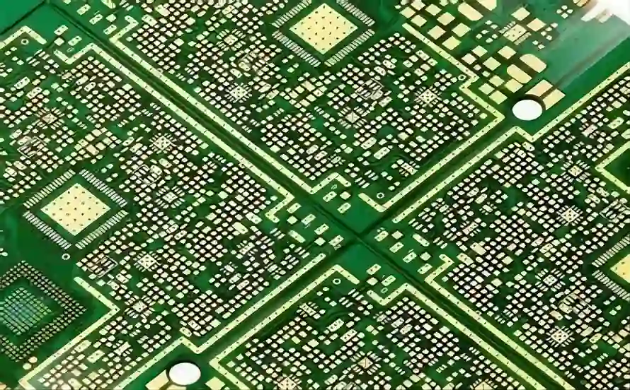
High-Density Interconnect (HDI) PCBs are specialized circuit boards designed to pack more components and connections into a smaller space compared to traditional PCBs. They achieve this through advanced manufacturing techniques and smaller features, such as microvias and fine lines, which allow for higher circuitry density. This compact design is crucial in applications where space is limited, and performance cannot be compromised—such as in CT scanners.
In CT scanners, HDI PCBs are used to manage complex signal processing, power distribution, and data transfer between various components like detectors, X-ray generators, and control systems. Their ability to handle high-speed signals—often in the range of several gigabits per second—and maintain signal integrity with low impedance (typically below 50 ohms for high-frequency lines) makes them indispensable. Without HDI technology, the compact and efficient design of modern CT scanners would be nearly impossible.
The Role of HDI PCBs in CT Scanners
CT scanners rely on a combination of mechanical, electrical, and digital systems to create detailed cross-sectional images of the human body. HDI PCBs are at the core of these systems, enabling several critical functions:
- Signal Processing: CT scanners generate massive amounts of data from X-ray detectors, often processing signals at speeds exceeding 1 Gbps. HDI PCBs ensure these signals are transmitted with minimal loss or interference.
- Compact Design: Space is a premium in medical devices. HDI PCBs allow for multi-layer designs—sometimes up to 12 or more layers—in a small footprint, fitting into tight enclosures within the scanner.
- Power Management: These boards handle high-voltage power distribution for X-ray tubes while maintaining stable low-voltage supplies for digital components, often managing currents up to 10 amps or more in specific circuits.
- Reliability: In a medical setting, failure is not an option. HDI PCBs are built to withstand constant operation, vibrations, and temperature fluctuations, ensuring consistent performance.
By leveraging high-density PCB manufacturing techniques, CT scanners can achieve faster scan times, higher image resolution, and improved patient safety through precise control systems.
Key Features of HDI PCB Design
HDI PCB design is defined by several advanced features that set it apart from standard circuit boards. Below, we’ll explore the most critical elements, including microvias, blind vias, buried vias, and laser drilling, and explain how they contribute to the functionality of CT scanners.
1. Microvias: The Backbone of High-Density Connections
Microvias are tiny holes, typically less than 150 micrometers in diameter, used to connect different layers of an HDI PCB. Unlike traditional through-hole vias that span the entire board, microvias are shallower and take up less space, allowing for denser layouts. In CT scanners, microvias enable the routing of high-speed signals between layers without introducing significant delays or crosstalk, maintaining signal integrity for data rates up to 10 Gbps in advanced systems.
Microvias are often created using laser drilling, a precise method that ensures clean, accurate holes. This technology is essential for fitting hundreds, if not thousands, of connections into the compact boards used in medical imaging equipment.
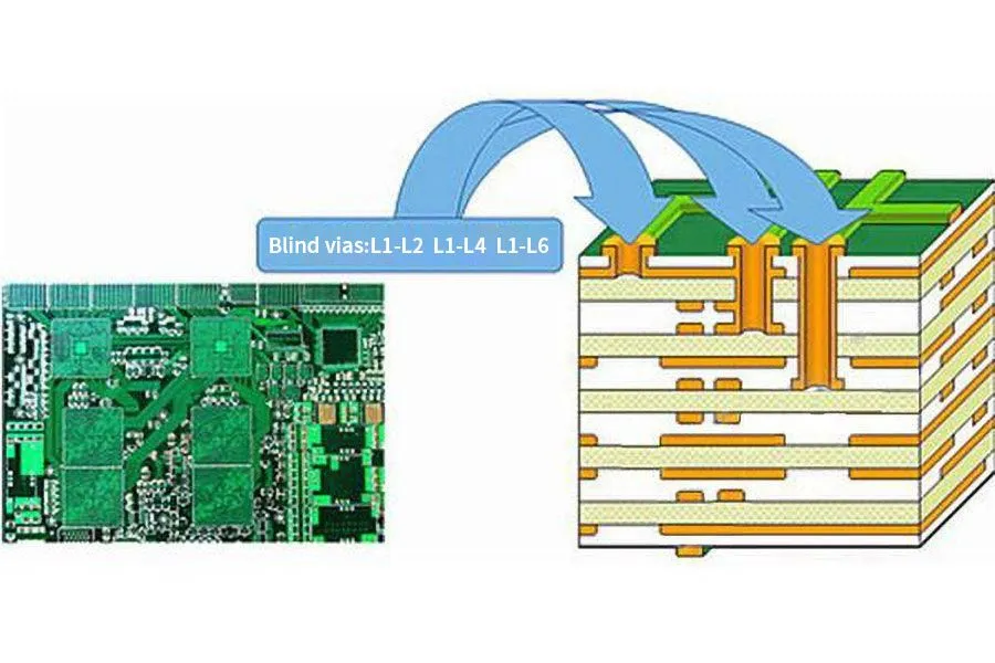
2. Blind Vias: Optimizing Space and Performance
Blind vias are connections that start on an outer layer of the PCB and terminate at an inner layer, without passing through the entire board. This design saves space on the opposite side of the board, allowing for more components or routing options. In CT scanners, blind vias are often used in areas where surface space is critical, such as near sensor arrays or control modules, enabling a denser component layout.
By reducing the number of through-hole vias, blind vias also minimize signal path lengths, which can lower impedance and improve performance for high-frequency signals—often achieving characteristic impedance values around 50 ohms for matched lines.
3. Buried Vias: Hidden Connections for Multi-Layer Designs
Buried vias connect internal layers of an HDI PCB without reaching the outer surfaces. These hidden connections are ideal for multi-layer boards, which are common in CT scanners due to their complexity. Buried vias free up surface space for additional components or traces, supporting the intricate circuitry needed for image processing and data transfer.
In high-density PCB manufacturing, buried vias are often used in conjunction with microvias to create a stacked or staggered structure, further increasing connection density. This approach is particularly useful in boards with 8 or more layers, where internal routing becomes a significant challenge.
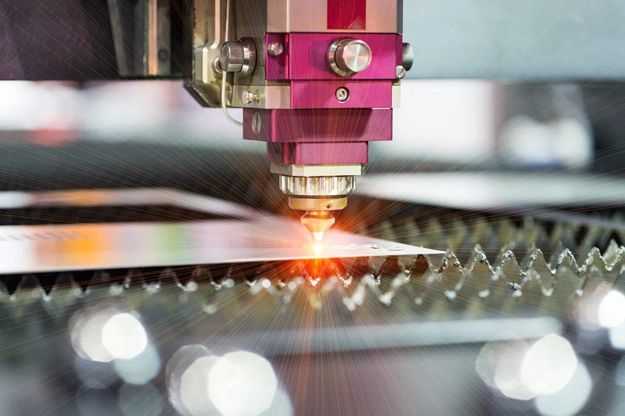
4. Laser Drilling: Precision in High-Density Manufacturing
Laser drilling is a cutting-edge technique used to create microvias, blind vias, and buried vias with extreme precision. Unlike mechanical drilling, which can be limited to larger hole sizes (typically above 0.2 mm), laser drilling can produce holes as small as 0.05 mm in diameter. This precision is vital for HDI PCB design, where every millimeter of space counts.
In the context of CT scanners, laser drilling ensures that the tiny vias needed for high-speed signal paths are formed accurately, reducing the risk of defects or signal degradation. The process also allows for faster production times, as modern laser systems can drill thousands of vias per second, supporting the demands of high-density PCB manufacturing.
Challenges in HDI PCB Manufacturing for CT Scanners
While HDI PCBs offer incredible benefits, their manufacturing process is far more complex than that of standard circuit boards. Here are some of the key challenges faced during high-density PCB manufacturing, especially for demanding applications like CT scanners:
- Tight Tolerances: HDI designs often require line widths and spacing as small as 0.075 mm (3 mils), demanding exceptional precision during fabrication and assembly. Even a slight deviation can lead to signal issues or board failure.
- Material Selection: High-frequency signals in CT scanners require materials with low dielectric loss, such as high-performance laminates with dielectric constants below 3.5. Choosing the right materials is critical to maintaining performance.
- Thermal Management: The compact nature of HDI PCBs can lead to heat buildup, especially in high-power sections of a CT scanner. Effective thermal vias and heat dissipation strategies are essential to prevent overheating.
- Cost: The advanced techniques involved in HDI PCB design, such as laser drilling and sequential lamination, increase production costs. Balancing cost with performance is a constant challenge for manufacturers.
Despite these hurdles, advancements in manufacturing technology continue to make HDI PCBs more accessible and reliable, ensuring they meet the rigorous demands of medical applications.
Benefits of HDI PCBs in Medical Imaging Equipment
The adoption of HDI PCBs in CT scanners and other medical imaging devices brings several tangible benefits that directly impact performance and patient outcomes:
- Enhanced Miniaturization: HDI technology allows for smaller, lighter devices, making CT scanners more portable and easier to integrate into hospital environments.
- Improved Signal Integrity: With shorter signal paths and reduced interference, HDI PCBs support faster data acquisition, leading to quicker scan times—often under 1 second per image in modern systems.
- Higher Reliability: The robust design and precise manufacturing of HDI PCBs ensure consistent operation, minimizing downtime in critical medical settings.
- Support for Advanced Features: HDI PCBs enable the integration of cutting-edge technologies, such as AI-driven image processing or real-time 3D reconstruction, directly into the scanner’s hardware.
These advantages highlight why HDI PCB design is not just a trend but a necessity in the evolution of medical imaging technology.
Future Trends in HDI PCB Technology for Medical Applications
As medical technology advances, so too does the role of HDI PCBs. Here are some emerging trends that could shape their use in future CT scanners:
- Increased Layer Counts: Future HDI PCBs may incorporate 16 or more layers to support even greater functionality in compact designs, driven by the need for more processing power.
- Advanced Materials: New substrates with ultra-low dielectric constants (below 2.5) and improved thermal properties are being developed to handle higher frequencies and heat loads.
- Automation in Manufacturing: Greater use of automated laser drilling and inspection systems will improve precision and reduce costs in high-density PCB manufacturing.
- Integration with IoT: HDI PCBs in CT scanners may soon include embedded sensors for real-time diagnostics and connectivity, enabling remote monitoring and predictive maintenance.
These innovations promise to make CT scanners faster, more efficient, and more accessible, further improving healthcare delivery worldwide.
Conclusion: The Power of HDI PCBs in Modern Healthcare
High-Density Interconnect (HDI) PCBs are a cornerstone of modern CT scanners, enabling the compact, high-performance designs needed to deliver precise medical imaging. Through advanced features like microvias, blind vias, buried vias, and laser drilling, HDI PCB design supports the complex requirements of signal processing, power management, and data transfer in these critical devices. The precision of high-density PCB manufacturing ensures that every component works seamlessly, contributing to faster diagnoses and better patient care.
As technology continues to evolve, HDI PCBs will remain at the forefront of medical innovation, driving improvements in performance, reliability, and accessibility. For engineers and manufacturers, understanding the intricacies of HDI technology is key to staying ahead in this fast-paced field. With the right design and manufacturing strategies, the potential of HDI PCBs in CT scanners is limitless, promising a future of even more advanced and efficient medical solutions.


