 ALLPCB


Are you struggling with heat dissipation in your high-power PCB designs? The via aspect ratio—a key design factor—plays a critical role in PCB thermal management. Simply put, the aspect ratio of a via (the ratio of its depth to its diameter) directly affects how efficiently heat is transferred away from hot components. In this blog, we’ll explore how via aspect ratio impacts thermal performance, dive into the role of thermal vias, and provide actionable insights for optimizing your high-power PCB design for better heat dissipation.
Introduction to PCB Thermal Management and Vias
In the world of electronics, managing heat is a top priority, especially for high-power PCB designs. As components like power transistors, LEDs, and processors generate significant heat, poor thermal management can lead to reduced performance, component failure, or even safety hazards. One of the most effective ways to tackle this issue is through the use of thermal vias—small, conductive pathways that transfer heat from the surface of the PCB to a heat sink or ground plane.
However, not all vias are created equal. The via aspect ratio, defined as the ratio of a via’s depth (or length through the board) to its diameter, has a profound impact on heat dissipation. A poorly designed aspect ratio can create thermal bottlenecks, while an optimized one can significantly enhance your board’s thermal performance. Let’s break down why this matters and how you can use it to your advantage in PCB thermal management.
What Is Via Aspect Ratio and Why Does It Matter?
The via aspect ratio is a simple yet critical metric in PCB design. It is calculated by dividing the depth of the via (how far it extends through the board) by its diameter (the width of the hole). For example, a via that is 1.6mm deep with a diameter of 0.3mm has an aspect ratio of approximately 5.3:1. This ratio influences both the manufacturing feasibility and the thermal performance of the via.
In terms of thermal management, the aspect ratio affects how much heat a via can conduct. A via with a high aspect ratio (long and narrow) may struggle to transfer heat effectively due to increased thermal resistance. On the other hand, a via with a low aspect ratio (short and wide) can often conduct heat more efficiently but may be limited by board thickness or design constraints. Understanding this balance is key to optimizing heat dissipation in high-power PCB designs.
Additionally, the aspect ratio impacts manufacturing. High aspect ratios can be challenging to plate with copper, leading to incomplete or uneven plating, which further reduces thermal conductivity. Striking the right balance is essential for both performance and producibility.
How Via Aspect Ratio Affects Heat Dissipation
Thermal vias work by providing a low-resistance path for heat to move from hot components to a cooler area, such as a ground plane or heat sink. The efficiency of this heat transfer depends heavily on the via’s design, including its aspect ratio. Here’s how it works:
- Thermal Resistance: A higher aspect ratio increases the length of the thermal path, which raises the thermal resistance of the via. This means less heat can flow through it per unit of time. For instance, a via with an aspect ratio of 10:1 may have a thermal resistance of around 50°C/W, while one with a 3:1 ratio could drop to 20°C/W, assuming similar materials and plating.
- Copper Plating Quality: During manufacturing, vias with high aspect ratios are harder to plate uniformly with copper. Incomplete plating reduces the effective cross-sectional area for heat conduction, further hampering performance.
- Heat Spreading: Vias with lower aspect ratios often allow better heat spreading across the board layers. This is particularly important in multilayer boards where heat needs to reach internal copper planes for dissipation.
For high-power PCB designs, where components might dissipate 10W or more, these factors can make a significant difference. A poorly designed via aspect ratio could result in temperature rises of 30°C or more at critical points, pushing components beyond their safe operating limits (often around 85-125°C for many ICs).
Optimizing Via Aspect Ratio for PCB Thermal Management
Now that we understand the relationship between via aspect ratio and heat dissipation, let’s look at practical ways to optimize it for better thermal performance. These strategies are especially useful for engineers working on high-power PCB designs where heat is a constant challenge.
1. Balance Aspect Ratio with Board Thickness
The thickness of your PCB directly impacts the via aspect ratio. For thicker boards (e.g., 2.4mm or more), achieving a low aspect ratio requires larger via diameters, which may not always be feasible due to space constraints. In such cases, consider using multiple smaller vias instead of a single large one. For example, replacing a single 0.5mm diameter via with four 0.3mm vias can reduce thermal resistance by up to 40% while keeping the aspect ratio manageable (around 5:1 or lower).
2. Use Via Arrays for High-Power Components
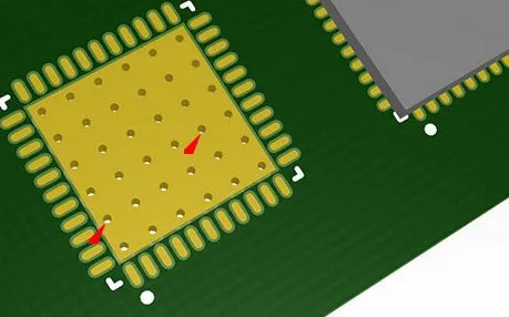
For components that generate significant heat, such as power MOSFETs or voltage regulators, place an array of thermal vias directly beneath or near the component’s thermal pad. A grid of vias with an aspect ratio of 3:1 to 5:1 can effectively transfer heat to a ground plane or heat sink. Studies have shown that a 3x3 grid of vias can reduce thermal resistance by 50-60% compared to a single via of the same total area.
3. Consider Via Fill Materials
Some designs benefit from filling thermal vias with conductive materials like epoxy or copper. This can lower thermal resistance, especially for vias with higher aspect ratios. Filled vias can improve heat transfer by up to 20%, though they increase manufacturing costs. Weigh the benefits against the budget for your project.
4. Simulate Thermal Performance
Before finalizing your design, use thermal simulation tools to model heat dissipation with different via aspect ratios. These tools can predict temperature rises at critical points, helping you choose the optimal via size and placement. For instance, a simulation might reveal that reducing the aspect ratio from 8:1 to 4:1 drops the junction temperature of a power IC from 110°C to 90°C, well within safe limits.
Challenges and Limitations of Via Aspect Ratio in Thermal Vias
While optimizing via aspect ratio is crucial for PCB thermal management, it’s not without challenges. Here are some common issues to keep in mind:
- Manufacturing Constraints: Most PCB fabrication processes have limits on aspect ratios, typically around 10:1 for standard boards. Pushing beyond this can lead to unreliable plating or even via failure, reducing thermal performance.
- Space Limitations: In densely packed high-power PCB designs, there may not be enough room to place large-diameter vias or arrays, forcing you to work with higher aspect ratios and accept reduced heat dissipation.
- Cost Considerations: Lowering the aspect ratio often means increasing via diameter or adding more vias, both of which can raise manufacturing costs. Balancing thermal needs with budget is a constant challenge.
Understanding these limitations helps set realistic expectations and guides trade-offs in your design process. Sometimes, combining thermal vias with other heat dissipation methods—like heat sinks or thicker copper layers—can compensate for less-than-ideal aspect ratios.
Best Practices for High-Power PCB Design and Thermal Management
Beyond optimizing via aspect ratio, effective thermal management in high-power PCB design requires a holistic approach. Here are some additional best practices to ensure your board stays cool under pressure:
- Increase Copper Thickness: Use heavier copper layers (e.g., 2oz or 3oz) to improve heat spreading across the board. Thicker copper can reduce thermal resistance by 30-50% compared to standard 1oz layers.
- Integrate Heat Sinks: Attach heat sinks directly to high-power components or connect them via thermal vias to pull heat away efficiently. Ensure the vias beneath the heat sink have an optimized aspect ratio for maximum heat transfer.
- Strategic Component Placement: Place heat-generating components away from each other to avoid creating hot spots. Distribute thermal vias evenly around these components to balance heat dissipation.
- Use Multilayer Boards: In multilayer designs, connect thermal vias to internal ground planes to spread heat across a larger area. This can lower temperatures by 10-20°C in critical areas.
By combining these techniques with careful attention to via aspect ratio, you can create high-power PCB designs that perform reliably even under demanding conditions.
Conclusion: Mastering Via Aspect Ratio for Better PCB Thermal Performance
In high-power PCB design, every detail counts when it comes to thermal management. The via aspect ratio, though often overlooked, is a critical factor in determining how effectively thermal vias can dissipate heat. By understanding its impact on thermal resistance, manufacturing feasibility, and overall heat dissipation, you can make informed decisions to optimize your designs.
Whether you’re working on a power supply, LED lighting system, or industrial controller, remember that a well-designed via aspect ratio—typically in the range of 3:1 to 5:1—can significantly reduce temperatures and improve reliability. Pair this with other thermal management strategies like via arrays, heavier copper, and simulations to ensure your PCB can handle the heat.


