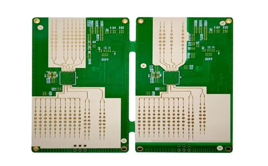
If you're dealing with a mobile phone that won't function due to damaged traces on its printed circuit board (PCB), don't worry. Repairing damaged traces on a mobile phone PCB is possible with the right tools, techniques, and a steady hand. This comprehensive guide will walk you through the process of PCB trace repair using methods like jumper wires, copper tape, and soldering techniques. Whether you're a hobbyist or a professional, you'll find actionable steps to get your device working again.
In the sections below, we'll dive deep into the world of PCB rework, covering everything from identifying damaged traces to applying advanced repair methods. Let's get started on restoring your mobile phone PCB to full functionality.
What Are PCB Traces and Why Do They Get Damaged?
PCB traces are thin lines of conductive material, usually copper, etched onto a circuit board to connect components like resistors, capacitors, and chips. In mobile phones, these traces are incredibly small and densely packed due to the compact design of modern devices. They carry electrical signals and power between components, ensuring the phone operates correctly.
Unfortunately, traces can get damaged due to several reasons:
- Physical Stress: Dropping a phone can crack or break traces on the PCB.
- Corrosion: Exposure to moisture or liquids can erode copper traces over time.
- Overheating: Excessive heat from components or poor design can weaken or burn traces.
- Manufacturing Defects: Some traces may have weak points from the production process, leading to failure under stress.
Damaged traces can cause issues like loss of power, no display, or failure of specific functions (e.g., touch not working). Repairing these traces is often more cost-effective than replacing the entire board, especially for high-end mobile phones.
Tools and Materials Needed for PCB Trace Repair
Before starting any PCB rework, gather the necessary tools and materials. Having everything ready will make the process smoother and reduce the risk of errors. Here's a list of essentials for repairing damaged traces on a mobile phone PCB:
- Soldering Iron: A fine-tip soldering iron (15-30W) for precise work on small traces.
- Solder Wire: Use thin, lead-free solder (0.5mm or smaller) for mobile phone repairs.
- Desoldering Wick: To remove old or excess solder from the board.
- Jumper Wires: Thin, insulated wires (30 AWG or smaller) to bridge broken traces.
- Copper Tape: Conductive tape to replace or reinforce damaged traces.
- Multimeter: To test continuity and identify broken traces.
- Magnifying Glass or Microscope: For inspecting tiny traces on mobile phone PCBs.
- Tweezers: Precision tweezers for handling small components and wires.
- Isopropyl Alcohol and Brush: To clean the PCB before and after repair.
- Flux: To improve solder flow and adhesion on traces.
- Heat-Resistant Mat: To protect your workspace from heat damage.
With these tools in hand, you're ready to tackle PCB trace repair. Always work in a well-lit, static-free environment to avoid further damage to the board.
Step-by-Step Guide to Repairing Damaged Traces on Mobile Phone PCBs
Repairing damaged traces on a mobile phone PCB requires patience and precision. Follow these steps carefully to ensure a successful repair. We'll cover multiple techniques, including jumper wire installation, copper tape application, and soldering methods for PCB rework.
Step 1: Inspect and Identify Damaged Traces
Start by visually inspecting the PCB under a magnifying glass or microscope. Look for visible cracks, burns, or breaks in the copper traces. Mobile phone PCBs often have traces as thin as 0.1mm, so magnification is crucial.
Use a multimeter set to continuity mode to confirm breaks. Place the probes on either end of a suspect trace. If there's no beep or reading, the trace is broken. Note the exact location of the damage for repair.
Tip: Traces near connectors, power lines, or high-heat areas (like near the CPU) are more prone to damage. Check these areas first.
Step 2: Clean the Damaged Area
Before any repair, clean the PCB to remove dirt, corrosion, or old solder. Dip a small brush in isopropyl alcohol (90% or higher) and gently scrub the damaged area. Avoid excessive pressure to prevent further damage to nearby traces or components.
Let the board dry completely before proceeding. A clean surface ensures better adhesion for solder or copper tape during PCB rework.
Step 3: Choose the Right Repair Technique
Depending on the extent of the damage and the trace's location, select the best repair method. Here are three common techniques for PCB trace repair on mobile phones:
Technique 1: Jumper Wire Repair
Jumper wires are ideal for bridging small breaks or connecting points across a damaged trace. This method works well when the trace can't be directly soldered or is in a hard-to-reach area.
- Cut a thin jumper wire (30 AWG) to the required length. Strip a small portion of insulation from both ends.
- Identify the two points on the trace that need to be connected. Scrape off any protective coating (solder mask) to expose the copper using a fine blade or sandpaper.
- Apply a small amount of flux to the exposed copper and tin it with a thin layer of solder.
- Position the jumper wire over the tinned points and solder it in place using a fine-tip soldering iron. Keep the soldering time under 2-3 seconds per point to avoid overheating.
- Test continuity with a multimeter to confirm the connection.
Note: Overheating can lift pads or damage nearby components. Use a soldering iron with temperature control set to around 300°C for mobile phone PCB rework.
Technique 2: Copper Tape Application
Copper tape is a quick solution for wider traces or when a direct replacement is needed. It's conductive and can be cut to size for precision repairs.
- Cut a small strip of copper tape slightly longer than the damaged trace section.
- Remove the backing and carefully place the tape over the damaged area, ensuring it aligns with the original trace path.
- Press down firmly to secure the tape. If necessary, use a small amount of conductive adhesive to hold it in place.
- Solder the ends of the copper tape to the existing trace for a strong electrical connection.
- Check continuity with a multimeter to verify the repair.
Tip: Copper tape works best for low-current traces. For high-current paths (like power lines), consider reinforcing with solder or a jumper wire.
Technique 3: Direct Soldering for Minor Breaks
For tiny cracks or breaks in traces, direct soldering can sometimes restore the connection without additional materials.
- Scrape off the solder mask over the damaged area to expose the copper trace.
- Apply flux to the break and use a fine-tip soldering iron to add a small amount of solder across the gap.
- Ensure the solder forms a smooth bridge without blobs or cold joints. Reheat if necessary to create a clean connection.
- Test the trace with a multimeter for continuity.
Caution: This method is only effective for very small breaks (less than 1mm). Larger gaps require jumper wires or copper tape.
Step 4: Test the Repair
After completing the repair, use a multimeter to confirm continuity across the repaired trace. Ensure there are no shorts with adjacent traces by testing nearby paths. If the phone powers on, check for functionality issues related to the repaired area (e.g., display, touch, or charging).
For complex mobile phone PCBs, signal integrity is critical. A poorly repaired trace can introduce impedance mismatches, affecting performance. For high-speed data lines (like USB or display signals), aim for repairs that maintain trace width and length as close to the original as possible. Typical impedance values for mobile phone data traces are around 50-90 ohms, so avoid excessive solder buildup or long jumper wires that could alter this.
Step 5: Secure and Protect the Repair
Once the repair is confirmed, protect the area to prevent future damage. Apply a thin layer of UV-curable solder mask or epoxy over the repaired trace to insulate it. This step is especially important for jumper wires, which can shift or break if not secured.
Ensure the protective coating doesn't interfere with nearby components or connectors. Let it cure fully before reassembling the phone.
Advanced Soldering Techniques for PCB Rework
For professionals or those comfortable with soldering, advanced techniques can improve the quality of PCB trace repair on mobile phones. Here are two methods to consider:
Drag Soldering for Fine Traces
Drag soldering involves using a small amount of solder and flux to create a smooth connection across a damaged trace. Apply flux to the area, load a small bead of solder on the iron tip, and drag it across the trace. This technique minimizes heat exposure and is ideal for traces near sensitive components.
Hot Air Rework for Component Protection
If the damaged trace is near surface-mount components, use a hot air rework station to avoid direct heat from a soldering iron. Set the station to a low temperature (around 250-300°C) and use a small nozzle to focus heat on the repair area. Combine with flux and solder wire for precise control.
Common Mistakes to Avoid During PCB Trace Repair
Repairing traces on a mobile phone PCB can be tricky, especially for beginners. Avoid these common pitfalls to ensure a successful repair:
- Overheating the Board: Excessive heat can lift pads or damage components. Limit soldering time to 2-3 seconds per point.
- Using Thick Wires or Tape: Oversized jumper wires or copper tape can cause shorts with nearby traces. Stick to thin, precise materials.
- Ignoring Signal Integrity: For high-speed traces, long jumper wires can introduce delays or interference. Keep repairs as short as possible.
- Skipping Cleaning: Dirt or residue can prevent solder from adhering properly, leading to weak connections.
- Not Testing: Always verify repairs with a multimeter before reassembling the phone to avoid hidden issues.
Preventing Future Damage to Mobile Phone PCBs
After repairing damaged traces, take steps to prevent recurrence. Handle the phone carefully to avoid drops or physical stress. Use a protective case to absorb impact. If the PCB was damaged by liquid, ensure the device is fully dried before powering on, and consider applying a conformal coating to protect against moisture.
For technicians, store PCBs in anti-static bags when not in use, and avoid working in humid environments that could lead to corrosion. Regularly inspect high-stress areas of the board during maintenance to catch issues early.
Conclusion
Repairing damaged traces on mobile phone PCBs is a valuable skill that can save you from costly replacements. By following this step-by-step guide, you can tackle PCB trace repair using jumper wires, copper tape, and advanced soldering techniques. Whether you're fixing a cracked trace or performing full PCB rework, precision and patience are key to success.
Armed with the right tools and methods, you can restore functionality to a damaged mobile phone PCB and extend the life of the device. Remember to test thoroughly after each repair and protect the board from future damage. With practice, PCB trace repair will become a straightforward task, empowering you to handle even the most complex mobile phone issues.
 ALLPCB


