ALLPCB


In the world of electronics, signal integrity is crucial for ensuring that high-speed circuits function reliably. But how do standard PCB dimensions affect signal integrity? Simply put, the size and layout of a printed circuit board (PCB) can directly influence signal quality through factors like trace length, impedance control, and interference. In this comprehensive guide, we’ll dive deep into how standard PCB sizes impact signal integrity, explore common issues, and provide actionable tips for optimizing your designs. Whether you're working on high-speed PCB design or tackling PCB signal integrity issues, this post will equip you with the knowledge you need.
Understanding Signal Integrity in PCB Design
Signal integrity refers to the ability of a signal to maintain its quality as it travels through a PCB. When signals degrade, it can lead to data errors, timing issues, or complete system failure. This is especially critical in high-speed PCB design, where signals operate at frequencies of hundreds of megahertz (MHz) or even gigahertz (GHz). Factors like crosstalk, reflections, and electromagnetic interference (EMI) can disrupt signal integrity, and the physical dimensions of a PCB play a significant role in managing these challenges.
Standard PCB dimensions—such as board thickness, width, and length—aren’t just about fitting components into a space. They influence trace routing, layer stackup, and impedance control, all of which are vital for maintaining clean signals. Let’s explore how these dimensions tie into PCB signal integrity issues and what you can do to address them.
How Standard PCB Sizes Impact Signal Integrity
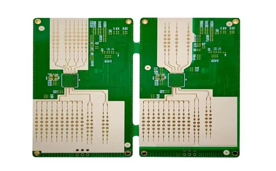
Standard PCB sizes are often determined by industry norms or specific application requirements. Common dimensions range from small boards (like 50mm x 50mm for compact devices) to larger ones (up to 500mm x 500mm for industrial systems). While these sizes are practical for manufacturing and assembly, they can introduce signal integrity challenges if not carefully considered during design.
1. Trace Length and Signal Delay
One of the most direct ways PCB dimensions affect signal integrity is through trace length. Larger boards often require longer traces to connect components, which can introduce signal delays. For high-speed signals, even a small delay can cause timing issues. For instance, at 1 GHz, a signal travels approximately 15 cm (6 inches) per nanosecond in a vacuum. On a PCB with a dielectric constant of 4.5 (common for FR-4 material), this speed drops to about 7 cm (2.8 inches) per nanosecond. A long trace on a large board could easily add unwanted delays, leading to signal misalignment.
To mitigate this, designers often need to minimize trace lengths by optimizing component placement. However, standard PCB sizes can limit how much you can shrink these paths, especially on larger boards with many components.
2. Impedance Control Challenges
PCB impedance control is critical for ensuring that signals travel without reflections. Impedance mismatches occur when the characteristic impedance of a trace doesn’t match the source or load impedance, often leading to signal distortion. Standard PCB dimensions influence impedance through trace width and board thickness, as these factors determine how traces interact with the dielectric material and ground planes.
For example, a typical 50-ohm impedance trace on a 1.6mm thick FR-4 board might require a trace width of about 0.3mm (12 mils) for a microstrip configuration. If the board thickness changes due to standard sizing constraints (e.g., using a thinner 0.8mm board for a compact design), the trace width must be adjusted to maintain the same impedance. Failing to account for this can result in signal reflections, especially in high-speed PCB design.
3. Crosstalk and EMI on Larger Boards
Larger standard PCB sizes often mean more components and longer, closely spaced traces, increasing the risk of crosstalk and EMI. Crosstalk happens when signals on adjacent traces interfere with each other, while EMI can be caused by external sources or poor grounding. Both issues degrade signal integrity and are more pronounced on bigger boards where traces may run parallel for longer distances.
For instance, if two traces are spaced less than 0.5mm apart on a large board, the coupling effect can induce unwanted noise, especially at high frequencies. Designers must balance the use of standard PCB sizes with proper trace spacing and shielding techniques to minimize these effects.
Key Factors in High-Speed PCB Design Related to Dimensions
High-speed PCB design amplifies the importance of dimensions due to the tight tolerances required for signal integrity. Let’s break down the critical elements tied to standard PCB sizes and how they influence performance.
PCB Trace Width and Current Capacity
Trace width is a fundamental aspect of PCB design that ties directly to both signal integrity and current-carrying capacity. Narrow traces are often needed for high-density designs on smaller standard PCB sizes, but they can increase resistance and inductance, leading to signal loss. Conversely, wider traces on larger boards reduce resistance but may not fit in compact layouts and can affect impedance.
A common rule of thumb is that a 1 oz copper trace with a width of 0.25mm (10 mils) can carry about 0.5A of current safely at room temperature. However, for high-speed signals, trace width must also be calculated based on impedance requirements, not just current. Using online calculators or simulation tools can help determine the optimal trace width for a given board thickness and dielectric constant.
Layer Stackup and Board Thickness
Standard PCB thicknesses (like 0.8mm, 1.6mm, or 2.4mm) affect how many layers you can include and how signals interact between them. Thicker boards allow for more layers, which can improve grounding and reduce EMI in high-speed designs. However, they also increase the distance between signal layers and ground planes, potentially affecting impedance and signal propagation.
For example, in a 4-layer board with a 1.6mm thickness, the distance between the top signal layer and the nearest ground plane might be 0.2mm, ensuring tight coupling and good signal integrity. Reducing the board to 0.8mm for a smaller design could halve this distance, requiring adjustments in trace width or dielectric material to maintain the same performance.
Common PCB Signal Integrity Issues Tied to Dimensions
Understanding the specific signal integrity issues caused by standard PCB sizes can help you design more reliable boards. Here are some frequent problems and their connection to dimensions.
Signal Reflections Due to Impedance Mismatch
As mentioned earlier, impedance mismatches cause signal reflections, which are more likely when board dimensions force trace widths or spacings outside ideal ranges. On a larger board, maintaining consistent impedance across long traces is harder, especially if the dielectric properties vary slightly due to manufacturing tolerances.
Timing Skew from Uneven Trace Lengths
On larger standard PCB sizes, it’s common for traces to have uneven lengths due to component placement. This leads to timing skew, where signals arrive at their destinations at different times. In high-speed designs, even a 1mm difference in trace length can cause a delay of several picoseconds, enough to disrupt data integrity at multi-GHz frequencies.
Power Distribution Challenges
Larger boards often require more complex power distribution networks (PDNs). If the board dimensions lead to long power traces or uneven ground planes, voltage drops and noise can affect signal integrity. Proper placement of decoupling capacitors near power pins is essential, but standard sizes may limit how close these components can be placed.
Practical Tips for Optimizing Signal Integrity with Standard PCB Sizes
While standard PCB dimensions can pose challenges, there are several strategies to maintain signal integrity in your designs. Here are actionable tips tailored for engineers working on high-speed PCB design.
1. Use Simulation Tools for Impedance Control
Before finalizing your design, use simulation software to model impedance based on your board’s dimensions and materials. Tools can predict how trace width, board thickness, and dielectric constants affect signal behavior, allowing you to adjust layouts for optimal performance.
2. Prioritize Component Placement
On larger boards, place critical components as close as possible to reduce trace lengths. Group high-speed components together to minimize signal delays and interference. Even with standard PCB sizes, strategic placement can significantly improve signal quality.
3. Implement Proper Grounding
A solid ground plane is essential for minimizing EMI and crosstalk. On larger boards, ensure the ground plane is continuous and covers as much area as possible. For multi-layer designs, dedicate entire layers to grounding to provide a low-impedance return path for signals.
4. Adjust Trace Width and Spacing
Calculate trace widths based on impedance requirements and ensure adequate spacing to prevent crosstalk. For high-speed signals, a spacing of at least three times the trace width is often recommended to reduce coupling effects.
Conclusion: Balancing Standard PCB Sizes with Signal Integrity
The impact of standard PCB dimensions on signal integrity cannot be overlooked, especially in high-speed PCB design. From trace length and impedance control to crosstalk and EMI, the size of your board influences every aspect of signal quality. By understanding these challenges and applying practical solutions like optimized trace width, strategic component placement, and robust grounding, you can mitigate PCB signal integrity issues and achieve reliable performance.
Designing with standard PCB sizes doesn’t have to mean compromising on quality. With careful planning and the right tools, you can turn dimensional constraints into opportunities for innovation. Keep these insights in mind as you tackle your next project, and ensure your designs deliver the speed and reliability your applications demand.