ALLPCB


PCB panel thickness is a critical factor that directly affects the manufacturing and assembly process of printed circuit boards. It influences everything from structural integrity to signal performance and assembly ease. Whether you're dealing with PCB panel warp, PCB panel bow, or ensuring the right PCB thickness for SMT (Surface Mount Technology), understanding and controlling panel thickness can make or break your project. In this comprehensive guide, we'll explore how PCB panel thickness impacts every stage of production and assembly, dive into PCB panel thickness tolerance, and provide actionable insights for achieving optimal results.
Why PCB Panel Thickness Matters
PCB panel thickness isn't just a number on a spec sheet; it’s a foundational element that determines how well a board performs mechanically and electrically. A board that’s too thin may bend or break under stress, while one that’s too thick can complicate assembly or increase costs unnecessarily. For engineers and manufacturers, choosing the right thickness is a balancing act between functionality, durability, and cost-efficiency.
Thickness affects key aspects such as:
- Mechanical stability during handling and assembly
- Thermal management and heat dissipation
- Signal integrity, especially in high-frequency applications
- Compatibility with assembly equipment, particularly for SMT processes
In the following sections, we'll break down these impacts in detail, focusing on how thickness ties into issues like warping, bowing, and tolerances.
Understanding PCB Panel Thickness and Standard Values
PCB panel thickness refers to the overall height of the board, including all layers of copper, substrate, and other materials. The most common standard thickness for PCBs is 1.6 mm (0.062 inches), which offers a good balance of strength and flexibility for many applications. However, depending on the project, thicknesses can range from as thin as 0.2 mm for flexible circuits to over 3.2 mm for heavy-duty boards used in industrial equipment.
Choosing the right thickness starts with understanding your application. For instance, thinner boards (0.8 mm or less) are often used in compact devices like smartphones, where space is limited. Thicker boards (2.0 mm or more) are preferred for applications requiring high durability, such as automotive or aerospace systems, where the board must withstand vibration and stress.
Manufacturers must also consider how thickness impacts the stack-up design. A multilayer board with a thickness of 1.6 mm might include 4 to 6 layers, with each layer contributing to the overall height. Deviations from standard thicknesses can lead to higher production costs since custom materials or processes may be required.
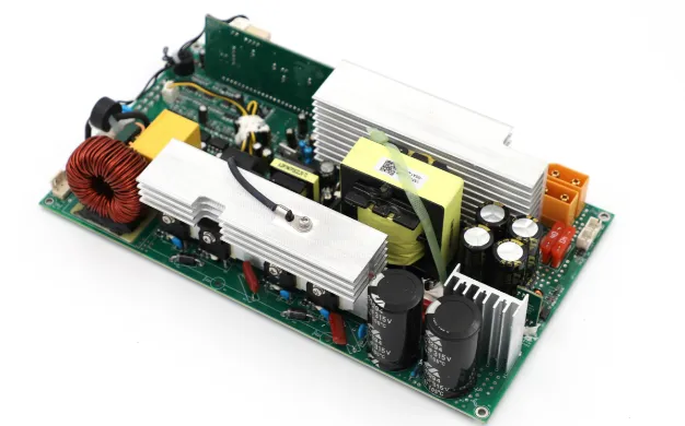
The Role of PCB Thickness in Manufacturing
During manufacturing, PCB panel thickness plays a significant role in determining how well the board holds up through various processes like drilling, etching, and lamination. Here’s how it impacts key stages:
1. Drilling and Via Formation
Thicker boards require more precise drilling equipment to create vias and through-holes. If the thickness exceeds the capabilities of standard machinery, it can lead to inaccuracies or damage to the board. For example, a board with a thickness of 2.4 mm might need specialized drills to ensure clean holes, increasing production time and cost.
2. Lamination and Layer Bonding
In multilayer boards, the lamination process bonds layers together under heat and pressure. If the panel thickness isn’t uniform or falls outside the expected range, uneven pressure can cause delamination or weak interlayer bonding. Maintaining tight PCB panel thickness tolerance (typically ±10% of the specified thickness) is crucial to avoid these issues.
3. Material Handling
Thinner panels (below 0.8 mm) are prone to bending or breaking during handling, especially in automated manufacturing lines. Conversely, thicker panels (above 2.0 mm) can be cumbersome and may not fit into standard equipment slots, requiring manual handling or custom setups.
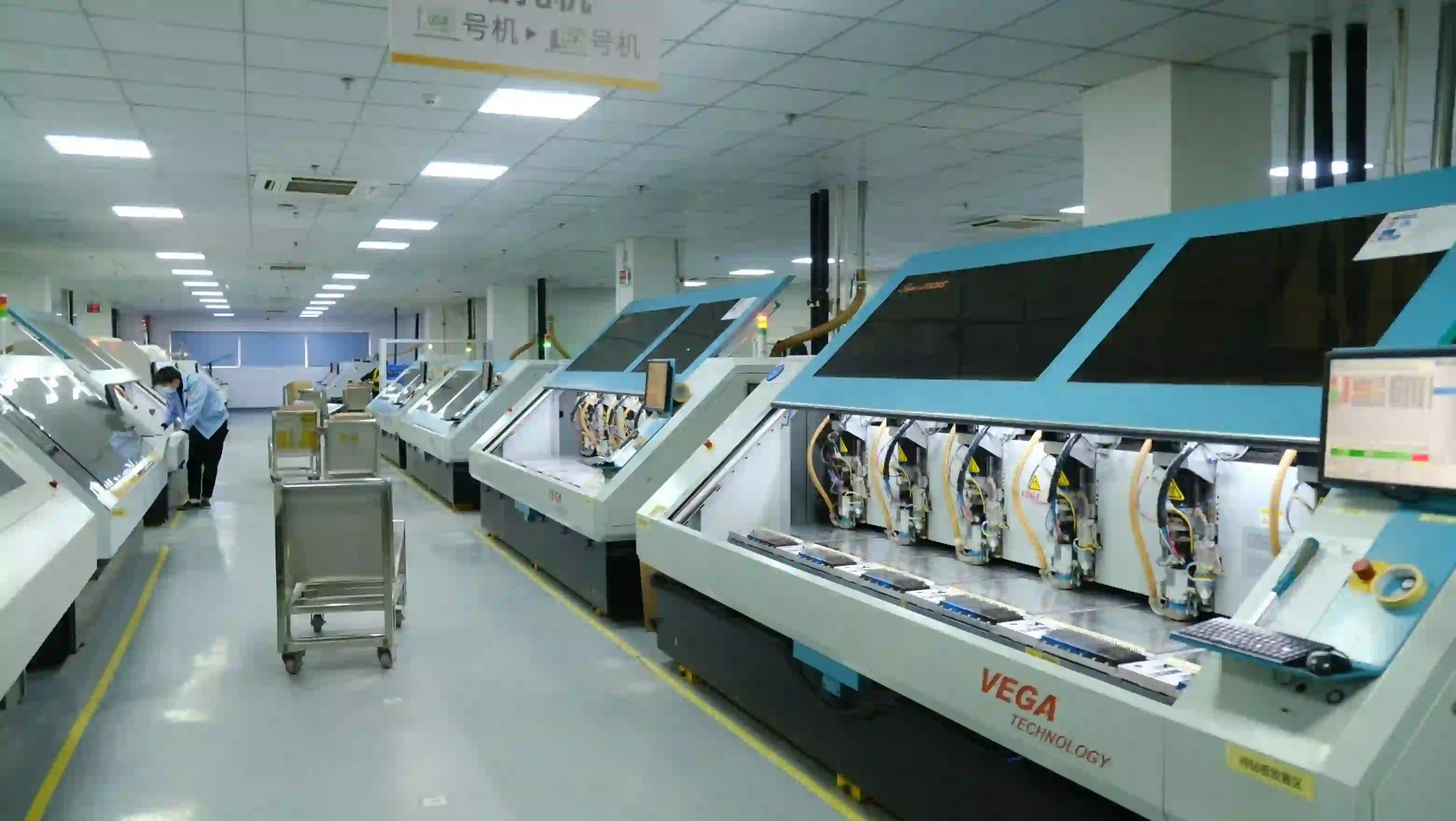
PCB Panel Thickness in Assembly: Focus on SMT
When it comes to assembly, particularly for PCB thickness for SMT, the panel thickness directly affects how components are placed and soldered onto the board. SMT assembly relies on precision, and any deviation in thickness can lead to defects. Here’s a closer look:
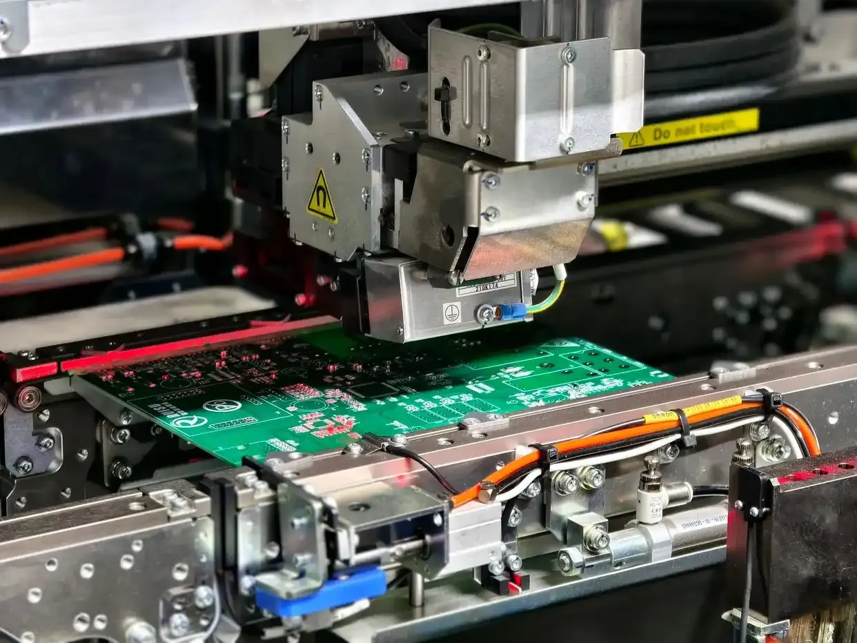
1. Component Placement Accuracy
SMT machines are calibrated for specific board thicknesses, typically around 1.6 mm. If a panel is too thin (e.g., 0.4 mm), it may flex during placement, causing misalignment of components. Thicker boards (e.g., 2.4 mm) might not fit into the machine’s clamps or require adjustments, slowing down the assembly process.
2. Soldering and Reflow
During the reflow soldering process, heat distribution is critical. Thicker boards absorb more heat, which can result in uneven soldering if the reflow profile isn’t adjusted. For instance, a 2.0 mm board may require a longer preheating phase compared to a 1.0 mm board to ensure proper solder joint formation. This is especially important to prevent issues like tombstoning, where components lift off the board due to uneven heating.
3. Compatibility with Stencils
Solder paste stencils used in SMT are designed for specific board thicknesses. A mismatch can lead to inconsistent paste application, causing defects like insufficient solder or bridging. Ensuring the panel thickness matches the stencil design is essential for high-quality assembly.
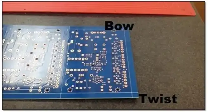
PCB Panel Warp and Bow: Causes and Solutions
Two common issues tied to PCB panel thickness are PCB panel warp and PCB panel bow. These deformations occur when a board isn’t flat, impacting both manufacturing and assembly. Let’s explore why they happen and how to mitigate them.
What Are Warp and Bow?
Warp refers to a twisting deformation along the diagonal of the panel, while bow describes a curvature along the length or width. Both are measured as a percentage of deviation from flatness. Industry standards, such as IPC-6012, typically allow a maximum warp and bow of 0.75% for SMT boards to ensure assembly reliability.
How Thickness Contributes to Warp and Bow
Thinner panels are more susceptible to warping due to their lack of rigidity. For example, a 0.6 mm board may warp under the high temperatures of reflow soldering (up to 260°C) if not properly supported. Thicker boards are less likely to deform but can still bow if there’s an imbalance in copper distribution between layers, causing uneven thermal expansion.
Preventing Warp and Bow
To minimize these issues, consider the following strategies:
- Use panelization techniques with evenly spaced breakaway tabs to reduce stress during depaneling.
- Balance copper distribution across layers to prevent uneven thermal expansion.
- Choose a thickness appropriate for the application—avoid going below 0.8 mm for boards exposed to high thermal stress.
- Store panels in a controlled environment to avoid moisture absorption, which can exacerbate warping.
PCB Panel Thickness Tolerance: Why Precision Matters
PCB panel thickness tolerance refers to the acceptable range of variation in a board’s thickness. Most manufacturers aim for a tolerance of ±10%, meaning a 1.6 mm board can range from 1.44 mm to 1.76 mm. However, tighter tolerances (e.g., ±5%) may be required for high-precision applications like RF circuits, where even small deviations can affect impedance.
Impact of Tolerance on Manufacturing
Loose tolerances can lead to issues like misalignment in multilayer stack-ups or inconsistent drilling depths. For example, if a board’s thickness varies by more than 0.2 mm across a panel, it can cause uneven pressure during lamination, resulting in weak bonding or voids.
Impact on Assembly
In assembly, thickness variations can disrupt automated processes. SMT pick-and-place machines rely on consistent board height for accurate component placement. A deviation of just 0.1 mm can lead to misaligned components or poor solder joints, increasing defect rates.
Achieving Tight Tolerances
To maintain tight tolerances, work closely with your manufacturing partner to specify material properties and process controls. Using high-quality substrates with consistent dielectric thickness (e.g., FR-4 with a dielectric constant of 4.5 at 1 MHz) can help. Additionally, regular quality checks during production ensure deviations are caught early.
How to Choose the Right PCB Panel Thickness
Selecting the optimal PCB panel thickness requires balancing several factors:
- Application Requirements: High-frequency designs may need thinner boards (0.8-1.0 mm) to minimize signal loss, while industrial applications often use thicker boards (2.0-3.2 mm) for durability.
- Assembly Process: For SMT, stick to standard thicknesses like 1.6 mm unless your equipment is calibrated for custom sizes.
- Cost Constraints: Thicker boards use more material, increasing costs. Non-standard thicknesses may also require custom tooling, adding to expenses.
- Thermal and Mechanical Stress: Boards exposed to high temperatures or vibration should be thicker to prevent PCB panel warp or cracking.
For most general-purpose applications, a thickness of 1.6 mm is a safe starting point. However, always consult with your design and manufacturing team to ensure the chosen thickness aligns with your project’s needs.
Conclusion: Mastering PCB Panel Thickness for Success
The impact of PCB panel thickness on manufacturing and assembly cannot be overstated. From preventing PCB panel warp and PCB panel bow to ensuring compatibility with PCB thickness for SMT, every decision about thickness influences the quality and reliability of the final product. By understanding factors like PCB panel thickness tolerance and applying best practices, you can avoid common pitfalls and achieve consistent, high-quality results.
Whether you're designing a compact consumer device or a robust industrial system, take the time to evaluate your panel thickness needs carefully. A well-chosen thickness not only improves manufacturability but also enhances the performance and longevity of your circuit boards. With the insights provided in this guide, you're equipped to make informed decisions that optimize both manufacturing and assembly processes.