 ALLPCB


Designing printed circuit boards (PCBs) for avionics systems is a complex task that demands precision and expertise. At the heart of this process lies the layer stack-up, a critical factor that directly impacts performance, signal integrity, and reliability in high-stakes aerospace applications. So, how do you optimize an avionics PCB layer stack-up for peak performance? The answer lies in carefully balancing impedance control, signal integrity, power distribution, and material selection to meet the stringent demands of avionics environments.
In this comprehensive guide, we'll dive deep into the art of layer stack-up design for avionics PCBs. We'll explore key considerations and best practices to help engineers achieve robust, high-performing designs that ensure safety and efficiency in the skies. Whether you're working on flight control systems, navigation equipment, or communication devices, this blog will provide actionable insights tailored to your needs.
Why Avionics PCB Layer Stack-Up Matters
Avionics systems operate in extreme conditions, from high altitudes to rapid temperature changes, while handling critical data and power requirements. A poorly designed PCB layer stack-up can lead to signal degradation, electromagnetic interference (EMI), or even system failure. Optimizing the avionics PCB layer stack-up is not just about performance—it's about ensuring the safety and reliability of aircraft operations.
A well-planned stack-up helps manage high-speed signals, minimizes noise, and ensures efficient power delivery. It also plays a vital role in meeting strict industry standards, such as those set by the Federal Aviation Administration (FAA) or the European Union Aviation Safety Agency (EASA). Let's break down the core elements of optimizing an avionics PCB layer stack-up and how they contribute to system performance.
Key Principles of Avionics PCB Layer Stack-Up Design
Creating an effective layer stack-up for avionics PCBs involves several key principles. Each layer must serve a specific purpose, and their arrangement must minimize interference while maximizing performance. Below, we explore the critical aspects of this design process.
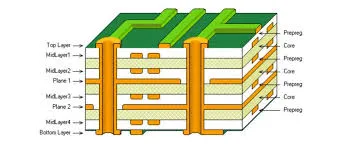
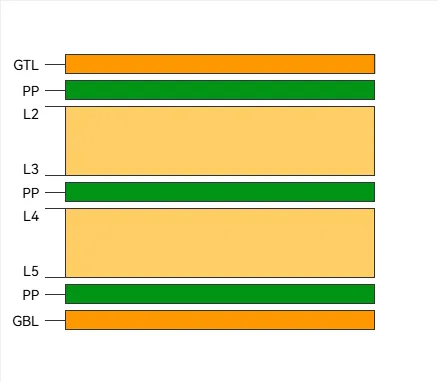
1. Layer Count and Arrangement in Avionics PCB Layer Stack-Up
The number of layers in a PCB depends on the complexity of the avionics system. Simple systems might use 4 to 6 layers, while advanced applications like radar or flight control systems often require 12 or more layers. A typical avionics PCB layer stack-up might include dedicated layers for signals, ground planes, and power distribution.
For example, in a 6-layer PCB, a common arrangement could be:
- Top Layer: High-speed signal traces
- Layer 2: Ground plane
- Layer 3: Power plane
- Layer 4: Power plane
- Layer 5: Ground plane
- Bottom Layer: Additional signal traces
This setup ensures that signal layers are sandwiched between ground planes, reducing EMI and crosstalk. Ground planes act as shields, while power planes provide stable voltage distribution. Proper layer ordering is crucial for maintaining signal integrity and minimizing noise in avionics systems.
2. Impedance Control in Avionics PCB Layer Stack-Up
Impedance control is a cornerstone of high-speed PCB design, especially in avionics where signals must travel without distortion. Impedance control in avionics PCB layer stack-up ensures that traces maintain consistent electrical characteristics, preventing reflections and signal loss.
For instance, a common target impedance for single-ended traces in avionics designs is 50 ohms, while differential pairs often aim for 90 to 100 ohms. Achieving this requires precise control over trace width, spacing, and the dielectric constant of the material between layers. A typical 1.6mm-thick PCB with a dielectric constant of 4.2 might require a trace width of 0.2mm for a 50-ohm impedance on outer layers.
To optimize impedance, designers often use simulation tools to model signal behavior before manufacturing. Placing ground planes close to signal layers reduces loop inductance and helps maintain consistent impedance across the board.
3. Signal Integrity in Avionics PCB Layer Stack-Up
Signal integrity is paramount in avionics, where even minor data corruption can have catastrophic consequences. Signal integrity in avionics PCB layer stack-up focuses on minimizing crosstalk, noise, and signal delays caused by improper layer design.
High-speed signals, such as those used in communication systems operating at 1 GHz or higher, are particularly vulnerable to interference. To protect them, designers should:
- Route critical signals on inner layers, shielded by ground planes.
- Avoid routing high-speed traces over splits in ground or power planes.
- Use controlled impedance traces to match the system's requirements.
Additionally, maintaining short trace lengths and using proper termination techniques can prevent signal reflections. For example, a signal traveling at 60% of the speed of light (a typical velocity factor in PCB materials) can experience significant delay over long traces, leading to timing errors in critical systems.
4. Power Distribution in Avionics PCB Layer Stack-Up
Efficient power delivery is essential for avionics systems, which often require multiple voltage levels for different components. Power distribution in avionics PCB layer stack-up focuses on minimizing voltage drops and ensuring stable current flow across the board.
Dedicated power planes are a common solution, as they provide low-impedance paths for current. For instance, a power plane designed for a 3.3V supply should be paired with a nearby ground plane to reduce inductance and noise. Designers should also use decoupling capacitors near power-hungry components to filter out high-frequency noise.
In a multi-layer design, splitting power planes into sections for different voltages (e.g., 5V, 3.3V, 1.8V) can help isolate noise. However, care must be taken to avoid creating gaps that disrupt return paths for signals, as this can lead to EMI issues.
5. Material Selection for Avionics PCB Layer Stack-Up
The choice of materials significantly impacts the performance of an avionics PCB. Material selection for avionics PCB layer stack-up must account for factors like dielectric constant, thermal stability, and mechanical durability to withstand the harsh conditions of aerospace environments.
Common materials include:
- FR-4: A cost-effective option for lower-frequency applications with a dielectric constant of around 4.2. However, it may not be suitable for high-speed designs due to higher signal loss.
- High-Tg FR-4: Offers better thermal stability for environments with temperature fluctuations, often exceeding 170°C glass transition temperature.
- Rogers Materials: High-frequency laminates with low dielectric constants (e.g., 3.0) and low loss tangents, ideal for radar and communication systems in avionics.
Selecting the right material also involves balancing cost and performance. For instance, while advanced laminates improve signal integrity at frequencies above 1 GHz, they can increase manufacturing costs. Engineers must evaluate the specific requirements of their avionics system to make an informed choice.
Best Practices for Optimizing Avionics PCB Layer Stack-Up
Beyond the core principles, several best practices can elevate the performance of your avionics PCB design. These tips are grounded in industry standards and real-world applications.
Minimize Layer Transitions for High-Speed Signals
Each time a signal changes layers through a via, it risks impedance mismatch and signal degradation. Limiting layer transitions and using back-drilling techniques to remove unused via stubs can improve signal integrity.
Use Symmetrical Stack-Ups
A symmetrical stack-up, where layers are balanced on either side of the board's center, helps prevent warping during manufacturing. For example, in an 8-layer PCB, ensure that the top and bottom halves mirror each other in terms of layer thickness and material.
Simulate and Test Designs
Before finalizing a design, use simulation software to analyze signal integrity, power distribution, and thermal performance. Tools can predict issues like crosstalk or voltage drops, allowing for adjustments early in the process. Post-manufacturing testing under simulated flight conditions is also critical for avionics PCBs.
Adhere to Industry Standards
Avionics PCBs must comply with standards like IPC-2221 for design and IPC-6012 for manufacturing. These guidelines ensure reliability and safety, covering aspects like minimum trace widths, via sizes, and material tolerances.
Challenges in Avionics PCB Layer Stack-Up Design
Designing an optimized layer stack-up for avionics systems comes with unique challenges. High-frequency signals, tight space constraints, and strict regulatory requirements can complicate the process. Additionally, the need to balance performance with cost often forces engineers to make tough trade-offs.
For instance, increasing the number of layers to improve signal isolation can raise manufacturing costs and board thickness, which may not be feasible in compact avionics enclosures. Similarly, using premium materials for better performance might strain project budgets.
To overcome these challenges, collaboration between design engineers, manufacturers, and material suppliers is essential. Early planning and iterative testing can also help identify and resolve issues before they escalate.
Conclusion: Mastering the Art of Avionics PCB Layer Stack-Up
Optimizing an avionics PCB layer stack-up is both a science and an art. It requires a deep understanding of impedance control, signal integrity, power distribution, and material selection to create designs that perform reliably under the demanding conditions of aerospace applications. By following the principles and best practices outlined in this guide, engineers can build robust PCBs that meet the highest standards of safety and efficiency.
From carefully arranging layers to selecting the right materials, every decision in the stack-up design process plays a role in the overall success of an avionics system. With the right approach, you can ensure that your PCB design not only meets technical requirements but also contributes to the safety and reliability of aircraft operations.
At ALLPCB, we’re committed to supporting engineers with the tools and expertise needed to bring their avionics designs to life. Whether you're tackling impedance control in avionics PCB layer stack-up or ensuring signal integrity in avionics PCB layer stack-up, our team is here to help you achieve outstanding results.


