 ALLPCB


In the fast-paced world of retail and payment processing, securing transactions is more critical than ever. Point-of-Sale (POS) systems handle sensitive data like credit card information, making them prime targets for tampering and hacking. So, how can you ensure your POS system is secure? The answer lies in robust PCB design tailored for security. This blog dives deep into POS PCB security design, anti-tampering PCB features, secure microcontroller integration, encryption module PCB layout, and PCI DSS compliant PCB design to help engineers and manufacturers build tamper-proof systems that protect transactions and customer trust.
Whether you're designing a new POS system or upgrading an existing one, this guide will walk you through actionable best practices to safeguard your hardware. Let’s explore how to create secure, reliable, and compliant designs that stand up to modern threats.
Why PCB Security Matters for Point-of-Sale Systems
POS systems are the backbone of retail transactions, processing millions of payments daily. However, their role in handling sensitive data makes them vulnerable to attacks like skimming, data theft, and physical tampering. A breach in a POS system can lead to financial losses, damaged reputation, and legal consequences. This is where POS PCB security design plays a pivotal role. A well-designed printed circuit board (PCB) acts as the first line of defense, protecting the hardware from unauthorized access and ensuring compliance with standards like PCI DSS (Payment Card Industry Data Security Standard).
By focusing on security during the PCB design phase, you can prevent costly redesigns and vulnerabilities down the line. Let’s break down the key elements of designing a tamper-proof POS system, starting with the foundational principles of security-focused PCB design.
Key Principles of POS PCB Security Design
Designing a secure PCB for a POS system requires a multi-layered approach that addresses both physical and digital threats. Here are the core principles to follow:
1. Layered Security Approach
Security isn’t a single feature—it’s a combination of multiple defenses. A layered approach includes physical barriers, encrypted data pathways, and tamper-detection mechanisms. For instance, integrating a secure microcontroller with hardware-based encryption ensures that even if one layer is breached, others remain intact. This reduces the risk of a single point of failure.
2. Compliance with PCI DSS Standards
PCI DSS is a set of security standards designed to protect cardholder data. A PCI DSS compliant PCB design must include features like encrypted communication channels and secure storage for sensitive information. Non-compliance can result in fines or loss of certification, so it’s crucial to design with these standards in mind from the start.
3. Focus on Physical and Digital Threats
POS systems face threats like physical tampering (e.g., drilling into the device to access components) and digital attacks (e.g., intercepting data signals). Your PCB design should address both by incorporating anti-tampering PCB features and secure data transmission protocols.
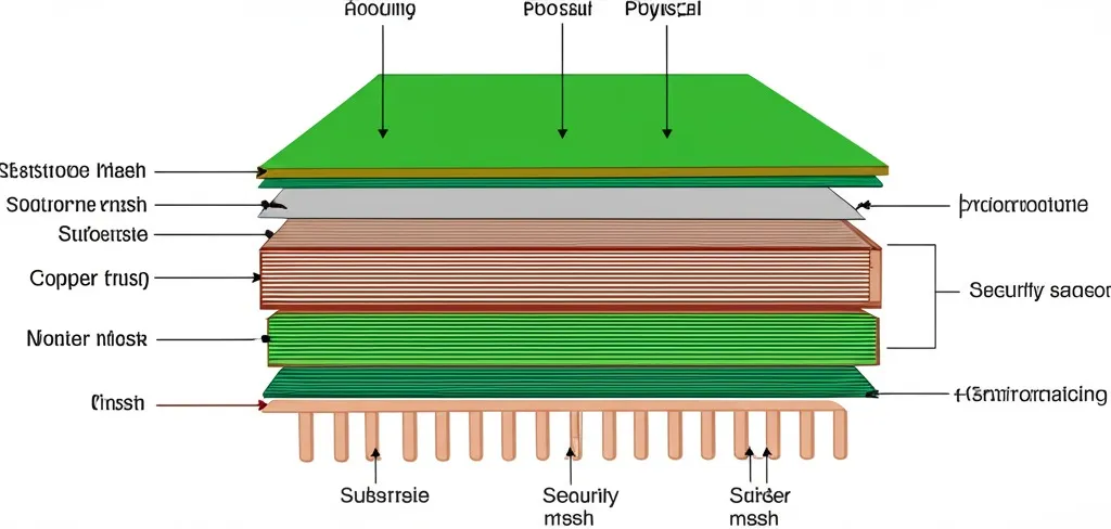
Anti-Tampering PCB Features for POS Systems
Physical tampering is a common attack vector for POS systems. Hackers may attempt to access internal components to extract data or install malicious hardware. Incorporating anti-tampering PCB features can deter or detect such attempts. Here are some proven strategies:
1. Tamper-Detection Sensors
Integrate sensors that detect unauthorized access, such as pressure or motion sensors. For example, a mesh layer on the PCB can trigger an alarm or wipe sensitive data if someone tries to drill through the board. These sensors should be connected to a secure microcontroller that logs or responds to tampering events.
2. Protective Coatings and Enclosures
Apply epoxy coatings or potting compounds over critical components to make reverse engineering difficult. These materials harden over the PCB, creating a physical barrier. Additionally, design the PCB to fit within a tamper-resistant enclosure with screws or seals that show evidence of tampering if disturbed.
3. Hidden Traces and Vias
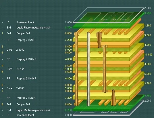
Design the PCB with buried traces and blind vias to hide critical signal paths. By placing sensitive data lines on inner layers of a multi-layer PCB (e.g., a 6-layer or 8-layer board), you make it harder for attackers to probe or intercept signals. Ensure that impedance for these traces is controlled, typically around 50 ohms for high-speed signals, to maintain signal integrity.
Secure Microcontroller Integration in POS PCB Design
The microcontroller is the brain of a POS system, handling data processing and communication. Integrating a secure microcontroller is essential to protect against firmware attacks and unauthorized access. Here’s how to do it effectively:
1. Choose a Microcontroller with Built-In Security
Select a microcontroller with hardware-based security features like secure boot, encrypted memory, and tamper detection. These features ensure that the firmware cannot be altered without authorization and that sensitive data is stored securely.
2. Isolate Critical Functions
Design the PCB to isolate the microcontroller from other components using dedicated power and ground planes. This reduces the risk of electromagnetic interference (EMI) and side-channel attacks, where attackers analyze power consumption to extract data. For instance, maintain a separation of at least 0.5 mm between sensitive traces and other signals to minimize crosstalk.
3. Implement Secure Firmware Updates
Allow firmware updates only through encrypted channels. Design the PCB to support a secure bootloader that verifies the authenticity of updates using digital signatures before installation. This prevents malicious code from being loaded onto the system.
Encryption Module PCB Layout for Data Protection
Encryption is a cornerstone of POS security, ensuring that sensitive data like cardholder information remains unreadable to unauthorized parties. A well-designed encryption module PCB layout is critical for effective data protection. Follow these best practices:
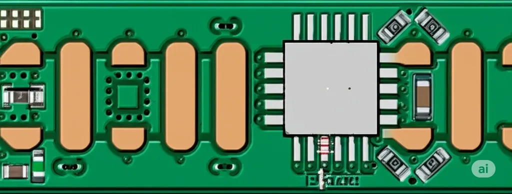
1. Dedicated Encryption Hardware
Use a dedicated encryption module or chip to handle data encryption and decryption. This offloads processing from the main microcontroller and enhances security by isolating cryptographic functions. Ensure the module supports strong algorithms like AES-256, which is widely used for securing payment data.
2. Minimize Signal Exposure
Place encryption-related traces on inner layers of the PCB to reduce the risk of signal interception. Keep trace lengths as short as possible—ideally under 10 mm for high-speed signals—to minimize electromagnetic radiation that could be picked up by attackers. Use differential signaling for critical data paths to further reduce noise and interference.
3. Secure Key Storage
Design the PCB to include secure storage for encryption keys, such as a hardware security module (HSM). Avoid storing keys in easily accessible memory locations. Physically separate the key storage area from other components, and use shielding to protect against electromagnetic attacks.
PCI DSS Compliant PCB Design: Meeting Industry Standards
Compliance with PCI DSS is non-negotiable for POS systems. A PCI DSS compliant PCB design ensures that your hardware meets the strict security requirements for handling payment data. Here are key considerations:
1. Secure Data Transmission
Design the PCB to support point-to-point encryption (P2PE), which encrypts data from the moment it’s entered until it reaches the payment processor. This minimizes the window of opportunity for data theft. Ensure that communication interfaces like USB or Ethernet are secured with proper shielding and filtering to prevent data leakage.
2. Physical Security Measures
PCI DSS requires physical protection against tampering. Incorporate tamper-evident designs, such as seals or labels that break if the device is opened. Additionally, ensure that all connectors and ports are secured or disabled if not in use to prevent unauthorized access.
3. Regular Security Testing
While not strictly a design element, PCB layouts should facilitate testing for vulnerabilities. Include test points for security audits, but ensure they are protected or disabled in production units to prevent exploitation. Work with third-party assessors to verify compliance during the design phase.
Additional Tips for Tamper-Proof POS PCB Design
Beyond the core elements, here are some additional tips to enhance the security of your POS PCB design:
- Power Supply Security: Use tamper-resistant power circuits to prevent attackers from cutting power to disable security features. Include backup power sources like capacitors to maintain critical functions during an attack.
- Thermal Management: Ensure proper heat dissipation for secure components. Overheating can degrade encryption modules or microcontrollers, so use heat sinks or thermal vias to maintain operating temperatures below 85°C.
- Documentation Control: Keep PCB design files and schematics secure. Limit access to authorized personnel only, and use encrypted file storage to prevent theft of intellectual property.
Challenges in Designing Secure POS PCBs
While implementing these best practices, engineers may face challenges like balancing security with cost, managing board space for additional features, and keeping up with evolving threats. To address these, prioritize critical security features based on risk assessments, and leverage modular designs to allow for future upgrades without a complete redesign.
For instance, a compact POS system may struggle with space for tamper-detection sensors. In such cases, opt for integrated solutions that combine multiple security features into a single chip or module, reducing the footprint while maintaining protection.
Conclusion: Building Trust Through Secure PCB Design
Designing a tamper-proof POS system starts with a security-first mindset at the PCB level. By focusing on POS PCB security design, incorporating anti-tampering PCB features, ensuring secure microcontroller integration, optimizing encryption module PCB layout, and adhering to PCI DSS compliant PCB design, you can create robust systems that protect transactions and build customer trust.
At ALLPCB, we understand the importance of secure hardware in today’s digital landscape. Our expertise in PCB manufacturing and assembly can help bring your secure POS designs to life with precision and reliability. By following the best practices outlined in this guide, you’re taking a significant step toward safeguarding sensitive data and ensuring compliance with industry standards. Let’s work together to secure every transaction, one PCB at a time.


