 ALLPCB


When designing a printed circuit board (PCB), one of the key considerations is how copper and matte solder mask interact to ensure reliable performance and manufacturability. For engineers and designers searching for insights on copper defined pads, mask defined pads, and related aspects like plating thicknesses and PCB design, understanding this relationship is crucial. In short, copper forms the conductive foundation of a circuit board, while a matte solder mask acts as a protective layer that prevents unwanted solder bridges and oxidation, with their contact points being critical for functionality.
In this comprehensive guide, we’ll dive deep into the interaction between copper and matte solder mask, exploring how they work together in PCB design. We’ll cover essential topics like pad definitions, plating processes, and even the role of materials like elastomer wires in modern circuits. Whether you’re a seasoned engineer or new to the field, this blog will provide actionable insights to enhance your designs.
What Are Copper and Matte Solder Mask in PCB Design?
In any circuit board, copper is the backbone of electrical conductivity. It forms the traces, vias, and pads that carry signals and power across the board. However, bare copper is prone to oxidation and can cause short circuits if solder accidentally bridges between components. This is where the solder mask comes in—a thin, protective layer applied over the copper to insulate it and prevent issues during assembly.
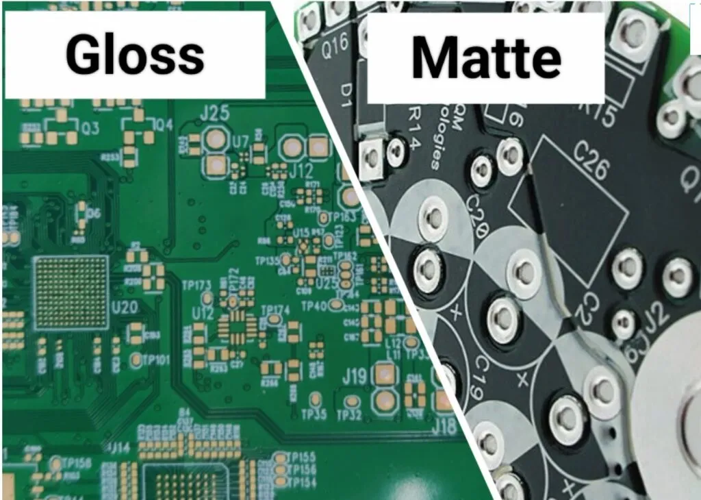
A matte solder mask, specifically, is a type of finish that reduces glare and provides a non-reflective surface. This makes it easier to inspect the board during manufacturing and assembly. The contact between copper and matte solder mask is carefully controlled to expose only the areas needed for soldering, such as pads, while protecting the rest of the copper traces. This balance is vital for both functionality and durability in PCB design.
Why Matte Solder Mask?
Matte solder masks are often preferred over glossy finishes in applications where visual inspection is critical. The lack of reflection helps automated optical inspection (AOI) systems detect defects more accurately. Additionally, matte finishes can offer better adhesion for certain types of components and coatings, making them a popular choice in high-reliability designs.
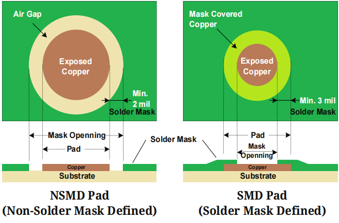
Understanding Copper Defined Pads and Mask Defined Pads
In PCB design, the way pads are created and exposed through the solder mask significantly impacts the board’s performance during assembly. Let’s break down the two primary types: copper defined pads and mask defined pads.
Copper Defined Pads
Copper defined pads are pads where the copper layer itself determines the final size and shape of the pad. The solder mask is applied with a slightly larger opening than the copper pad, ensuring that the entire pad is exposed for soldering. This method is often used in high-density designs where precision is critical, as it minimizes the risk of mask misalignment affecting the pad area.
For example, in a design with fine-pitch components, copper defined pads ensure that the pad size remains consistent, even if the solder mask shifts slightly during manufacturing. This approach is ideal for surface-mount technology (SMT) components with tight tolerances.
Mask Defined Pads
On the other hand, mask defined pads rely on the solder mask opening to define the size of the exposed copper area. The copper beneath the mask is larger than the opening, so the mask effectively limits the solderable area. This method is common in designs where controlling solder spread is essential, as the mask acts as a barrier to prevent excess solder from flowing onto adjacent areas.
Mask defined pads are often used for through-hole components or in designs where larger pads are needed for mechanical strength. However, they can be more susceptible to issues if the mask is misaligned during production.
The Role of Plating Thicknesses in Copper and Solder Mask Contact
Another critical factor in how copper interacts with matte solder mask is the plating thicknesses applied to the exposed copper areas. Plating, often done with materials like tin, nickel, or gold, protects the copper from oxidation and enhances solderability. The thickness of this plating can affect both the electrical performance and the physical durability of the pads.
Common Plating Thicknesses
In most circuit board designs, plating thicknesses vary based on the application. For instance:
- Electroless Nickel Immersion Gold (ENIG): Typically, nickel plating ranges from 3 to 6 micrometers, with a thin gold layer of 0.05 to 0.1 micrometers on top. This finish is common in high-reliability applications due to its corrosion resistance.
- Hot Air Solder Leveling (HASL): This process results in a tin-lead or lead-free solder layer, usually 1 to 25 micrometers thick, depending on the board’s requirements. HASL is cost-effective but less suitable for fine-pitch components.
- Immersion Tin: Often around 0.8 to 1.2 micrometers, immersion tin provides a flat surface for SMT components but has a shorter shelf life due to potential oxidation.
The choice of plating thickness impacts how well the copper withstands environmental factors and how effectively it bonds with solder during assembly. If the plating is too thin, it may not protect the copper adequately, leading to oxidation beneath the matte solder mask. If it’s too thick, it can increase costs and affect the pad’s flatness, complicating assembly.
How Matte Solder Mask Affects Copper Contact Points
The matte solder mask’s primary role is to insulate copper traces and prevent solder from adhering to unwanted areas. However, its interaction with copper at contact points—such as pads and vias—must be carefully managed during PCB design to avoid issues like solder mask encroachment or insufficient coverage.
Preventing Solder Mask Encroachment
Solder mask encroachment happens when the mask partially covers the edge of a pad, reducing the solderable area. This can lead to weak solder joints or assembly failures. To prevent this, designers often specify a solder mask clearance (the distance between the edge of the pad and the mask opening) of at least 0.05 to 0.1 mm, depending on the manufacturing capabilities.
Ensuring Proper Coverage
On the flip side, insufficient solder mask coverage can expose copper traces, leading to short circuits or corrosion. A well-designed matte solder mask should cover all non-solderable areas while leaving precise openings for pads and vias. The matte finish also helps reduce errors during inspection, as it minimizes reflections that could obscure defects.
Elastomer Wires in PCB Design: A Modern Consideration
While copper and solder mask form the core of most circuit board designs, modern applications sometimes incorporate specialized materials like elastomer wires. These flexible, conductive materials are often used in wearable electronics or flexible PCBs, where traditional copper traces may not provide the necessary durability under repeated bending or stretching.
Elastomer wires can be integrated into a PCB alongside copper traces, with the matte solder mask protecting both materials from environmental damage. However, designers must consider how the mask adheres to elastomer materials, as their flexibility can sometimes cause delamination if not properly managed. Specialized adhesives or mask formulations may be required to ensure a secure bond.
For example, in a wearable device with a strain of up to 50% during use, elastomer wires might replace copper in high-flex areas, while a matte solder mask provides insulation. This hybrid approach balances conductivity and flexibility, showcasing the versatility of modern PCB design.
Best Practices for Designing Copper and Matte Solder Mask Contact
To achieve optimal performance in your circuit board, follow these best practices when designing the interaction between copper and matte solder mask:
- Define Pad Types Early: Decide whether to use copper defined pads or mask defined pads based on your component types and assembly requirements. For fine-pitch SMT components, copper defined pads often provide better precision.
- Specify Plating Thicknesses: Work with your manufacturer to choose the right plating thicknesses for your application. For high-reliability designs, consider ENIG with a nickel layer of 4-5 micrometers and a gold layer of 0.08 micrometers.
- Optimize Solder Mask Clearance: Ensure a clearance of at least 0.05 mm between the solder mask and pad edges to prevent encroachment while maintaining coverage over traces.
- Account for Material Properties: If using innovative materials like elastomer wires, test the adhesion of the matte solder mask to avoid delamination in flexible or high-stress applications.
- Leverage Matte Finish for Inspection: Use the non-reflective properties of matte solder mask to improve AOI accuracy during manufacturing, reducing the risk of undetected defects.
Common Challenges and Solutions in Copper and Matte Solder Mask Contact
Even with careful planning, challenges can arise when designing the contact between copper and matte solder mask. Here are a few common issues and how to address them:
- Misalignment of Solder Mask: This can expose unintended copper or cover pad areas. Solution: Use tighter manufacturing tolerances and verify mask alignment during prototyping.
- Plating Wear: Thin or poor-quality plating can wear off, exposing copper to oxidation. Solution: Specify appropriate plating thicknesses and choose finishes suited to your environment (e.g., ENIG for harsh conditions).
- Solder Bridging: Excess solder can bridge between pads if mask openings are too large. Solution: Refine mask openings and consider mask defined pads for better control over solder spread.
Conclusion: Mastering Copper and Matte Solder Mask Contact in PCB Design
The relationship between copper and matte solder mask is a cornerstone of effective PCB design. By understanding concepts like copper defined pads, mask defined pads, and plating thicknesses, designers can create circuit boards that are both reliable and manufacturable. Incorporating modern elements like elastomer wires further expands the possibilities for innovative designs, provided the interaction with solder mask is carefully managed.
With the actionable tips and detailed insights provided in this guide, you’re equipped to optimize the contact points between copper and matte solder mask in your next project. From specifying pad types to choosing the right plating, every decision plays a role in ensuring the success of your design. Keep these principles in mind, and you’ll be well on your way to creating high-quality PCBs that meet the demands of today’s technology.


