 ALLPCB


Designing a PCB outline and stencil is crucial for accurate solder paste application in surface mount technology (SMT) assembly. A well-thought-out PCB outline stencil ensures that solder paste is applied precisely where it’s needed, preventing issues like bridging or insufficient solder joints. In this comprehensive guide, we’ll explore the essentials of PCB outline stencil design, including aperture considerations and best practices for solder paste application, to help you achieve flawless SMT assembly results. Whether you’re focusing on PCB outline solder paste techniques or optimizing a PCB outline aperture, this blog will provide actionable insights for engineers and manufacturers.
Why PCB Outline and Stencil Design Matter for SMT Assembly
The PCB outline and stencil design are foundational to the SMT assembly process. The stencil, often made of thin stainless steel, acts as a template for applying solder paste onto the PCB’s surface mount pads. If the PCB outline stencil isn’t designed with precision, you risk uneven paste application, which can lead to defective solder joints or component misalignment. A poorly designed PCB outline aperture can also cause issues like excess paste or insufficient coverage, impacting the reliability of the final product.
In SMT assembly, accuracy is everything. Studies show that up to 60% of soldering defects stem from improper solder paste application. By focusing on PCB outline solder paste techniques and stencil design, you can significantly reduce these errors, saving time and costs in production.
Understanding the Basics of PCB Outline Stencil Design
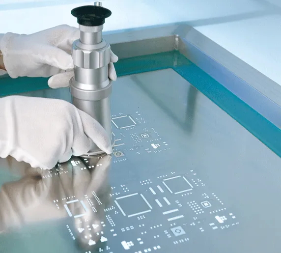
A PCB outline stencil is a tool used to deposit solder paste onto specific areas of a PCB during assembly. The stencil features openings, or apertures, that correspond to the pads on the PCB where components will be placed. These apertures are typically created using laser-cutting technology to ensure high precision, often achieving tolerances as tight as ±0.005 mm.
When designing a PCB outline stencil, several factors must be considered:
- Material Thickness: Stencils are usually made from stainless steel with thicknesses ranging from 0.1 mm to 0.2 mm, depending on the component sizes and paste volume required.
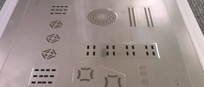
- Aperture Size and Shape: The PCB outline aperture must match the pad dimensions on the PCB. For fine-pitch components, such as those with a 0.4 mm pitch, smaller apertures are necessary to avoid excess paste.
- Alignment: The stencil must align perfectly with the PCB outline to ensure accurate paste deposition. Misalignment by even 0.05 mm can cause soldering defects.
By optimizing these elements, you ensure that the PCB SMT stencil design supports consistent and reliable solder paste application, minimizing rework in the assembly process.
Key Elements of PCB Outline Aperture Design
The PCB outline aperture is arguably the most critical aspect of stencil design. Apertures determine how much solder paste is applied to each pad, directly affecting the quality of the solder joint. Here are some key considerations for designing effective apertures:
1. Aperture-to-Pad Ratio
The size of the aperture should generally be slightly smaller than the pad size to prevent excess paste. A common rule of thumb is to design apertures at 90% of the pad area for standard components. For finer pitch components (below 0.5 mm), this ratio may drop to 80% to avoid bridging.
2. Aspect Ratio for Paste Release
The aspect ratio, defined as the aperture width divided by the stencil thickness, should ideally be above 1.5 to ensure proper paste release. For example, if your stencil is 0.15 mm thick, the aperture width should be at least 0.225 mm to prevent paste from sticking to the stencil walls.
3. Shape Adjustments for Specific Components
For components like QFNs (Quad Flat No-leads), stencil apertures often include a "windowpane" design, where the aperture is split into smaller segments to reduce the risk of voiding during reflow soldering. This technique can reduce voiding rates by up to 30% compared to a single large aperture.
Best Practices for PCB Outline Solder Paste Application
Once the PCB outline stencil is designed, the next step is applying solder paste accurately. Proper application techniques are just as important as the stencil itself. Here’s how to ensure precision during this critical stage of SMT assembly:
1. Use the Right Solder Paste
Solder paste consists of tiny metal particles suspended in flux, and its composition affects application quality. For most SMT applications, a Type 3 or Type 4 paste (particle sizes of 25-45 μm or 20-38 μm, respectively) works well. Finer pastes are better for smaller apertures, ensuring smoother deposition through the PCB outline stencil.
2. Control Squeegee Pressure and Speed
During application, a squeegee pushes solder paste through the stencil apertures. Too much pressure can cause paste to bleed under the stencil, while too little pressure results in incomplete filling. A typical squeegee pressure ranges from 0.3 to 0.5 kg/cm2, with a speed of 20-40 mm/s for optimal results.
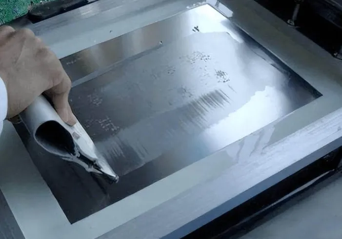
3. Maintain Stencil Cleanliness
Residual paste on the stencil can clog apertures, leading to uneven application. Clean the stencil after every 5-10 prints using an alcohol-based cleaner and a lint-free wipe. Automated under-stencil cleaning systems can further improve consistency in high-volume production.
Common Challenges in PCB SMT Stencil Design and Solutions
Even with careful planning, challenges can arise during PCB SMT stencil design and solder paste application. Here are some common issues and how to address them:
1. Solder Paste Bridging
Bridging occurs when excess paste connects adjacent pads, often due to oversized apertures or high squeegee pressure. To prevent this, reduce aperture size by 10-15% for fine-pitch components and adjust squeegee settings to minimize paste overflow.
2. Insufficient Solder Paste
If too little paste is applied, solder joints may be weak or incomplete. This can result from clogged apertures or a low aspect ratio. Ensure regular stencil cleaning and verify that the aspect ratio meets the minimum threshold of 1.5.
3. Stencil Misalignment
Misalignment between the stencil and PCB outline can shift paste deposition, causing component placement errors. Use fiducial marks on both the PCB and stencil for precise alignment, and consider automated stencil printers for high-accuracy production.
Advanced Techniques for Optimizing PCB Outline Stencil Design
For engineers looking to take their PCB SMT stencil design to the next level, advanced techniques can further improve accuracy and efficiency:
1. Step Stencils for Mixed Component Sizes
In designs with both large and small components, a single stencil thickness may not suffice. Step stencils feature varying thicknesses—thicker areas for larger components needing more paste (e.g., 0.2 mm) and thinner areas for fine-pitch components (e.g., 0.1 mm). This approach can reduce defects by up to 25% in mixed assemblies.
2. Nano-Coatings for Improved Paste Release
Applying a nano-coating to the stencil surface can enhance paste release, especially for ultra-fine apertures below 0.3 mm in width. These coatings reduce friction, ensuring cleaner paste deposition and extending stencil lifespan by up to 20%.
3. Simulation Software for Design Validation
Before manufacturing a stencil, use simulation tools to model solder paste behavior based on aperture size and stencil thickness. These tools can predict potential issues like bridging or insufficient paste, allowing for design adjustments before production begins.
The Role of PCB Outline in Overall Stencil Effectiveness
The PCB outline itself plays a significant role in stencil design and solder paste application. The outline defines the board’s shape and dimensions, which must be mirrored in the stencil for proper alignment. Any discrepancy between the PCB outline and stencil frame can lead to misalignment during printing.
For non-standard board shapes, such as circular or irregular outlines, custom stencil frames may be necessary to ensure stability during paste application. Additionally, incorporating tooling holes or slots in the PCB outline design can aid in securing the board during assembly, reducing movement and improving accuracy.
How to Choose the Right Stencil for Your Project
Selecting the appropriate PCB outline stencil depends on your project’s specific requirements. Here are some factors to consider:
- Production Volume: For low-volume or prototype runs, a frameless stencil is often sufficient and cost-effective. High-volume production benefits from framed stencils compatible with automated printers.
- Component Density: High-density designs with fine-pitch components require thinner stencils (0.1-0.12 mm) and smaller apertures for precision.
- Budget Constraints: While advanced options like step stencils or nano-coatings improve performance, they come at a higher cost. Balance performance needs with budget limitations.
Conclusion: Achieving Precision with PCB Outline and Stencil Design
Accurate solder paste application is the cornerstone of successful SMT assembly, and it starts with a well-designed PCB outline stencil. By focusing on critical elements like PCB outline aperture sizing, material thickness, and application techniques, you can minimize defects and ensure reliable solder joints. Whether you’re refining PCB outline solder paste methods or exploring advanced stencil technologies, attention to detail in PCB SMT stencil design will pay off in improved product quality and production efficiency.
With the insights and best practices shared in this guide, you’re equipped to tackle the challenges of stencil design and solder paste application. A small investment in precision at this stage can lead to significant gains in the overall success of your PCB assembly process.


