 ALLPCB


In the fast-evolving world of electronics, High-Density Interconnect (HDI) PCBs are at the forefront of enabling smaller, faster, and more efficient devices. A critical aspect of HDI PCB manufacturing is panel size optimization, which directly impacts cost, efficiency, and performance. If you're wondering how to choose the right HDI PCB panel size or manage challenges like microvia panelization and panel size for fine-pitch components, this guide is for you. We'll dive deep into the strategies and considerations for optimizing panel sizes in high-density PCB manufacturing, covering everything from stackup design to laser via drilling.
This comprehensive guide will walk you through the essentials of panel size optimization for HDI PCBs, providing actionable insights and practical tips to ensure your designs meet performance and cost goals. Let’s explore the key factors that influence panel size decisions and how to navigate the complexities of HDI manufacturing.
What is Panel Size Optimization in HDI PCB Manufacturing?
Panel size optimization refers to the process of determining the most efficient dimensions of a PCB panel—the larger board that holds multiple individual PCBs during manufacturing. For HDI PCBs, which feature intricate designs with high wiring density, microvias, and fine-pitch components, choosing the right panel size is crucial. It affects production yield, material usage, and overall costs in high-density PCB manufacturing.
HDI PCBs are defined by their compact layouts and advanced interconnect technologies, often incorporating blind and buried vias. Unlike traditional PCBs, HDI designs require precise planning to balance the number of boards per panel with manufacturing constraints. A well-optimized HDI PCB panel size maximizes the number of usable boards while minimizing waste and ensuring compatibility with fabrication equipment.
Why Panel Size Matters for HDI PCBs
The panel size you choose for HDI PCB production influences several critical factors:
- Cost Efficiency: Larger panels can accommodate more individual boards, reducing per-unit costs. However, oversized panels may lead to material waste if not fully utilized.
- Manufacturing Compatibility: Equipment limitations, such as the maximum panel size a fabricator can handle, dictate feasible dimensions.
- Yield and Reliability: Proper panelization ensures uniform processing, reducing defects during steps like laser via drilling panel considerations.
- Design Constraints: HDI PCBs often involve fine-pitch components and dense layouts, requiring careful spacing and alignment on the panel to avoid signal integrity issues.
Optimizing panel size is not just about fitting as many boards as possible; it’s about striking a balance between efficiency and quality. Let’s break down the key considerations for achieving this balance.
Key Factors in HDI PCB Panel Size Optimization
1. Understanding HDI Stackup Design
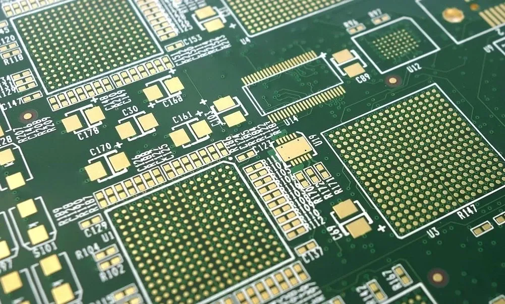
The HDI stackup design is the foundation of any high-density PCB. It defines the arrangement of copper layers, dielectric materials, and vias (including microvias) within the board. Stackup design directly impacts panel size because it determines the complexity of manufacturing processes and the space required for each board.
For instance, an HDI board with a 6-layer stackup, including 2 build-up layers on each side, might require specific panel spacing to accommodate sequential lamination processes. If microvias are stacked across multiple layers, additional precision is needed during panelization to ensure alignment. A common stackup for HDI designs might include a total thickness of 1.6mm, with microvia aspect ratios of 0.8:1 for reliability.
When optimizing panel size, ensure that the stackup design is compatible with the panel’s dimensions. Overcrowding a panel can lead to misalignment during lamination, while underutilizing space increases costs. Always collaborate with your fabrication team to confirm that the panel size supports the intended HDI stackup design.
2. Microvia Panelization Challenges
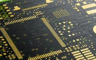
Microvia panelization is a critical step in HDI PCB manufacturing. Microvias are tiny vias, often with diameters as small as 0.1mm, used to connect layers in a compact space. These vias are typically formed using laser drilling, which requires precise alignment across the panel.
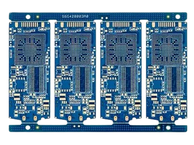
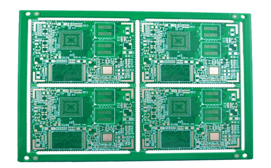
During panelization, the placement of individual boards must account for the laser drilling process. Uneven spacing or improper panel size can lead to inconsistent via formation, affecting electrical performance. For example, a panel that is too large may exceed the laser drilling machine’s working area, while a panel that is too small may not justify production costs. A standard panel size for HDI boards with microvias is often around 18x24 inches, though this varies based on fabricator capabilities.
To optimize microvia panelization, consider using software tools to simulate panel layouts. These tools can help identify the best arrangement to maximize board count while ensuring uniform via placement.
3. Laser Via Drilling Panel Considerations
Laser via drilling panel considerations are vital for HDI PCB production. Laser drilling is used to create microvias with high precision, often achieving diameters below 0.15mm. However, the process is sensitive to panel size and material uniformity.
Larger panels can pose challenges for laser drilling equipment, as maintaining focus and accuracy over a wide area becomes difficult. Conversely, smaller panels may reduce throughput, increasing production time. A practical approach is to design panels within the equipment’s optimal working area, typically between 12x18 inches and 24x30 inches for most modern laser systems.
Additionally, ensure that the panel material is consistent to avoid variations in drilling depth. For HDI PCBs, materials like high-Tg FR-4 or polyimide are often used to withstand the thermal stress of laser drilling. Proper panel size planning can minimize defects like incomplete vias or over-drilling, which can compromise signal integrity.
4. Panel Size for Fine-Pitch Components
HDI PCBs are often used in applications with fine-pitch components, such as BGA (Ball Grid Array) packages with pitches as small as 0.4mm. The panel size for fine-pitch components must account for the tight tolerances required during assembly.
If the panel is too large, warpage or uneven heating during reflow soldering can misalign components. On the other hand, a panel that is too small may not provide enough space for proper tooling rails or fiducial marks, which are essential for precise component placement. A balanced panel size, often around 18x24 inches for medium-complexity HDI designs, can accommodate fine-pitch assembly while maintaining stability.
Tip: Include extra spacing between individual boards on the panel to allow for precise pick-and-place operations. This reduces the risk of errors when placing components with tight tolerances.
Best Practices for High-Density PCB Manufacturing
In high-density PCB manufacturing, panel size optimization is just one piece of the puzzle. Here are some best practices to ensure success throughout the production process:
1. Collaborate Early with Fabricators
Before finalizing your panel size, work closely with your manufacturing partner. They can provide insights into equipment limitations, standard panel sizes, and material availability. Early collaboration helps avoid costly redesigns and ensures that your HDI PCB panel size aligns with production capabilities.
2. Use Panelization Software
Advanced software tools can simulate panel layouts, helping you maximize board count while adhering to design rules. These tools are especially useful for complex HDI designs with microvias and fine-pitch components, as they can identify potential issues before production begins.
3. Account for Material Shrinkage
During manufacturing, materials like FR-4 can shrink by up to 0.5% due to heat and pressure. Factor this into your panel size calculations to avoid misalignment of vias or components. For HDI PCBs, where precision is critical, even small deviations can lead to failures.
4. Optimize for Yield
Design your panel to minimize waste while maximizing the number of usable boards. For example, arrange boards in a grid pattern with minimal spacing, but leave enough room for cutting and handling. A well-optimized panel might achieve a yield of 90% or higher, significantly reducing costs.
Common Challenges in HDI PCB Panel Optimization
Even with careful planning, challenges can arise during panel size optimization for HDI PCBs. Here are some common issues and how to address them:
- Equipment Limitations: If your panel size exceeds the fabricator’s capabilities, consider splitting the design into smaller panels or adjusting the layout. Standard panel sizes often range from 18x24 inches to 24x36 inches.
- Signal Integrity Risks: Overcrowding a panel can lead to crosstalk or impedance mismatches, especially in HDI designs with high-speed signals. Maintain controlled impedance, targeting values like 50 ohms for single-ended traces, by spacing boards appropriately.
- Thermal Stress: Large panels may experience uneven heating during soldering, causing warpage. Use materials with low thermal expansion coefficients and design panels to distribute heat evenly.
Conclusion: Achieving Efficiency with HDI PCB Panel Size Optimization
Panel size optimization is a critical step in the design and manufacturing of High-Density Interconnect (HDI) PCBs. By carefully considering factors like HDI stackup design, microvia panelization, laser via drilling panel considerations, and the needs of fine-pitch components, you can achieve a balance between cost efficiency and performance in high-density PCB manufacturing.
Start by understanding your design requirements and collaborating with your fabrication team to choose the right HDI PCB panel size. Use software tools to simulate layouts, account for material properties, and follow best practices to maximize yield. With these strategies, you’ll be well-equipped to navigate the complexities of HDI PCB production and deliver high-quality, reliable boards for your applications.
Whether you’re working on compact consumer electronics or advanced industrial systems, optimizing panel size ensures that your HDI PCBs meet the demands of modern technology. Take the time to plan thoroughly, and you’ll see the benefits in reduced costs, improved quality, and faster time-to-market.


