ALLPCB


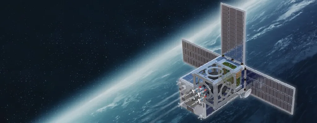
In the high-stakes world of satellite payload design, outgassing from printed circuit boards (PCBs) poses a significant challenge. Outgassing, the release of volatile organic compounds (VOCs) and other gases from materials in a vacuum environment, can lead to contamination, degraded performance, and even mission failure. For engineers working on satellite payloads, understanding how to tackle outgassing through careful material selection and effective mitigation strategies is critical. This blog dives deep into the issue, focusing on low-outgassing PCB materials, designing for a vacuum environment, adhering to NASA outgassing standards, and ensuring contamination control in space.
Whether you're an aerospace engineer or a PCB designer new to space applications, this guide offers practical insights and actionable steps to minimize outgassing risks in your satellite payload projects. Let's explore the science behind outgassing, its impact on satellite systems, and the best practices to address these challenges.
What Is Outgassing and Why Does It Matter for Satellite Payload PCBs?
Outgassing refers to the process where materials release trapped gases, moisture, or volatile organic compounds when exposed to a vacuum or high-temperature environment, such as space. In satellite payload PCBs, outgassing can create serious problems. The released gases can condense on sensitive components like optical sensors, lenses, or solar panels, forming a thin film that impairs their functionality. This contamination can reduce signal clarity, distort measurements, or even cause electrical shorts in critical systems.
In a vacuum environment, there's no atmosphere to dissipate these gases, so they linger and interact with nearby surfaces. For satellite payloads, where precision and reliability are non-negotiable, even small amounts of contamination from volatile organic compounds in PCBs can jeopardize a mission costing millions of dollars. Therefore, controlling outgassing is a top priority for space-grade electronics.
The Impact of Outgassing on Satellite Payload Performance
The effects of outgassing in a vacuum environment for PCBs are far-reaching. Here are some specific ways it impacts satellite payload performance:
- Contamination of Optical Systems: Volatile organic compounds released from PCB materials can deposit on lenses and mirrors, reducing their reflectivity or transparency. For instance, a study by space agencies has shown that even a 1% reduction in optical clarity can skew data collection by up to 5% in imaging systems.
- Degradation of Thermal Control: Outgassed materials can alter the thermal properties of surfaces, affecting the satellite's ability to manage heat. This is critical since space systems often operate in extreme temperature ranges from -150°C to 150°C.
- Electrical Interference: Condensed gases can create conductive paths on PCB surfaces, leading to short circuits or signal interference. This is especially problematic for high-frequency signals in communication payloads where impedance mismatches can degrade performance by 10-20%.
- Mechanical Stress: Outgassing can cause material expansion or contraction in confined spaces, leading to mechanical stress or delamination in multilayer PCBs.
These risks highlight why outgassing must be addressed during the design and manufacturing phases of satellite payload PCBs. Let's look at how material selection plays a pivotal role in minimizing these issues.
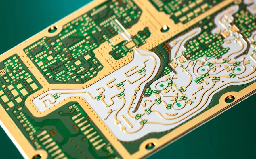
Choosing Low-Outgassing PCB Materials for Space Applications
Selecting the right materials is the first line of defense against outgassing in a vacuum environment for PCBs. Not all standard PCB substrates and coatings are suitable for space use, as many contain high levels of volatile organic compounds. Here’s a breakdown of key considerations and recommended low-outgassing PCB materials:
Key Material Properties to Consider
- Total Mass Loss (TML): This measures the percentage of a material’s mass lost due to outgassing under vacuum conditions. Materials for space applications should have a TML of less than 1%.
- Collected Volatile Condensable Material (CVCM): This indicates the amount of outgassed material that condenses on nearby surfaces. A CVCM of less than 0.1% is ideal for space-grade PCBs.
- Thermal Stability: Materials must withstand extreme temperature fluctuations without releasing gases or degrading.
Recommended Low-Outgassing PCB Materials
- Polyimide Laminates: Known for their thermal stability and low TML (often below 0.5%), polyimide-based materials are widely used in space applications. They can handle temperatures up to 260°C without significant outgassing.
- PTFE-Based Materials: Polytetrafluoroethylene (PTFE) composites offer low dielectric constants and minimal outgassing, making them suitable for high-frequency satellite communication payloads. Their CVCM values are typically below 0.05%.
- Ceramic-Filled Laminates: These materials provide excellent thermal and mechanical stability with TML values as low as 0.2%. They are often used in high-reliability applications.
- Conformal Coatings: Silicone-based or parylene coatings can be applied to PCBs to reduce outgassing from exposed surfaces. Parylene, in particular, has a CVCM of less than 0.01%.
By prioritizing low-outgassing PCB materials, engineers can significantly reduce the risk of contamination in space. However, material selection alone isn't enough. Compliance with established standards is equally important.
Understanding NASA Outgassing Standards for PCB Design
For space-bound electronics, adhering to NASA outgassing standards is a must. These standards provide a framework for evaluating and selecting materials to ensure minimal contamination risk. The primary reference for outgassing data is NASA's Outgassing Database, maintained by the Goddard Space Flight Center. Here's what you need to know:
NASA SP-R-0022A Guidelines
NASA's SP-R-0022A specification outlines the test methods and acceptance criteria for materials used in space. The standard testing procedure, ASTM E595, measures TML and CVCM under controlled vacuum and temperature conditions (typically 125°C for 24 hours). Materials passing these tests are listed in NASA's database for reference.
- TML Limit: Less than 1.0% mass loss.
- CVCM Limit: Less than 0.1% condensable material.
Why Compliance Matters
Non-compliance with NASA outgassing standards can lead to mission delays or failures. For instance, a material with a high CVCM might pass initial tests but cause contamination over a multi-year mission, degrading critical systems. Using pre-tested, NASA-approved materials ensures long-term reliability in the harsh vacuum environment of space.
Accessing Outgassing Data
Engineers can refer to NASA's online outgassing database for detailed material data. This resource, updated regularly, includes test results for thousands of materials, helping designers make informed choices for satellite payload PCBs.
Contamination Control in Space: Beyond Material Selection
While low-outgassing PCB materials and adherence to NASA standards form the foundation of outgassing control, additional strategies are necessary for comprehensive contamination control in space. Here are proven mitigation techniques:
Pre-Baking PCBs
Pre-baking involves heating PCBs in a vacuum chamber before assembly to drive out trapped moisture and volatile compounds. A typical pre-bake process might involve temperatures of 100-120°C for 24-48 hours. This can reduce outgassing by up to 50%, based on industry studies.
Ventilation Design
Incorporating vent holes or channels in PCB enclosures allows gases to escape without condensing on sensitive components. For example, spacing vent holes every 5-10 cm on a payload enclosure can improve gas dissipation in vacuum conditions.
Component Selection
Beyond PCB substrates, components like capacitors, resistors, and IC packages must also be evaluated for outgassing. Opt for ceramic-packaged components over plastic ones, as they release fewer volatile organic compounds. Ceramic packages often have TML values below 0.3% compared to 2-3% for plastic equivalents.
Cleanroom Assembly
Assembling PCBs in a controlled cleanroom environment minimizes the introduction of contaminants like dust or organic residues, which can contribute to outgassing. ISO Class 5 or better cleanrooms are recommended for space-grade electronics.
Design Considerations for Vacuum Environment PCBs
Designing PCBs for a vacuum environment requires more than just material selection. The layout and structure of the board must account for the unique challenges of space. Here are some key design tips:
- Minimize Exposed Surfaces: Reduce the surface area of materials prone to outgassing by using conformal coatings or encapsulating components. This can cut down VOC release by up to 30%.
- Avoid Adhesives: Many adhesives have high outgassing rates. If unavoidable, choose space-rated, low-VOC adhesives with TML below 0.5%.
- Optimize Layer Stackup: Use fewer layers where possible to reduce the volume of material that could outgas. For a 6-layer board, ensure inner layers use the same low-outgassing substrate as outer layers.
- Thermal Management: Design for efficient heat dissipation to prevent localized hot spots that could accelerate outgassing. Incorporate thermal vias with a diameter of 0.3-0.5 mm to channel heat away from critical areas.
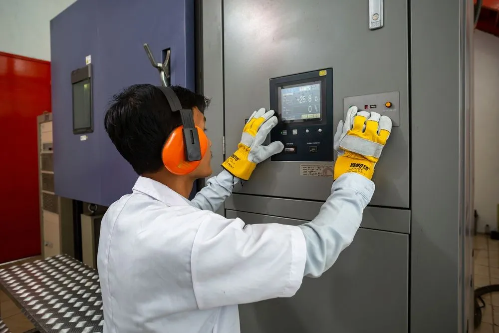
Testing and Validation for Outgassing Control
Once a PCB is designed and assembled, rigorous testing is essential to validate its performance in a vacuum environment. Here are common testing methods:
- ASTM E595 Testing: As mentioned earlier, this standard test measures TML and CVCM. It’s a benchmark for space-grade materials and should be conducted on both raw materials and finished PCBs.
- Thermal Vacuum Testing: Simulates space conditions by exposing the PCB to vacuum and temperature cycles (e.g., -100°C to 100°C). This helps identify potential outgassing issues over time.
- Residual Gas Analysis (RGA): Uses mass spectrometry to detect and analyze gases released from the PCB in a vacuum chamber. RGA can pinpoint specific volatile organic compounds for targeted mitigation.
Testing data should be documented and compared against mission requirements. For instance, if a satellite mission spans 10 years, ensure that outgassing rates remain within acceptable limits for the entire duration.
Conclusion: Building Reliable Satellite Payload PCBs
Outgassing challenges in satellite payload PCBs are a complex but manageable issue. By focusing on low-outgassing PCB materials, adhering to NASA outgassing standards, and implementing robust mitigation strategies, engineers can minimize the risks of contamination control in space. From selecting polyimide or PTFE-based substrates to pre-baking boards and designing for a vacuum environment, every step counts in ensuring mission success.
At the heart of reliable satellite design is the understanding that even small amounts of volatile organic compounds in PCBs can have outsized impacts. With the right materials, design practices, and testing protocols, you can build PCBs that withstand the harsh conditions of space and deliver consistent performance over long missions. Stay informed, prioritize quality, and keep pushing the boundaries of space technology with confidence.